As I mentioned in the previous post, the soul of the ZX Spectrum 48K microcomputer—what a surprise—is the Z80 CPU. Obviously, you need to emulate the CPU to get closer to a full Spectrum emulator. Believe it or not, CPU emulation is not a big challenge compared to other devices of the machine (video display generation, tape emulation, etc.), but it is laborious due to the richness of Z80’s instruction set.
Before going into the implementation details I used in SpectNetIde, I give you a brief overview of Z80A. Please, do not expect this article as a tutorial to learn about the CPU. I will focus on the aspects that are the most essential from the emulator design and development point of view.
The manufacturer of Z80A, Zilog, is an American manufacturer of microcontrollers. Its most known product is the Z80 family of chips. According to its simplicity from hardware interfacing point of view, it became popular right after its initial issue in 1976.
The Z80A version—the one used in ZX Spectrum 48K—is an improved model that increased the maximum speed of the original Z80 from 2.5 MHz to 4 MHz. The chip is an 8-bit CPU with 8-bit and 16-bit registers and provides over 1000 instructions.
Registers As Figure 1 depicts, it has 8 main registers (A, B, C, D, E, H, L, and F) with their corresponding alternate registers (A’, B’, C’, D’, E’, H’, L’, and F’); two index registers (IX, IY); a stack pointer (SP); a program counter (PC), and two special registers, I and R.
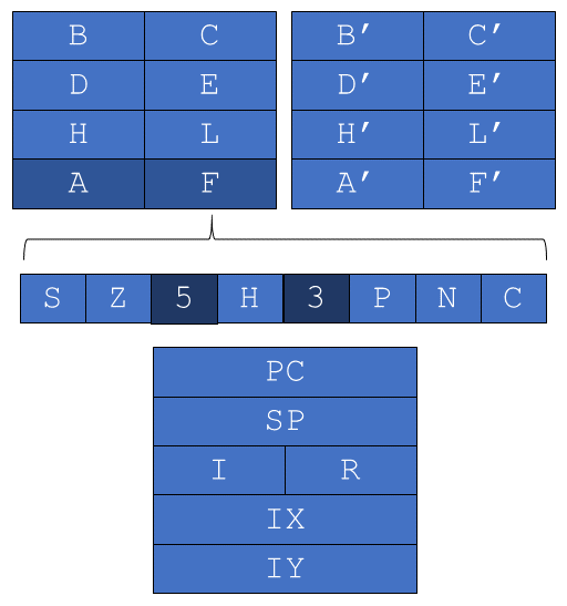
Figure 1: The registers of the Z80A CPU
The A register is called Accumulator. From the programming point of view, this register is the most flexible, as it can be the operand of more instructions than any others. The F register is a set of 1-bit flags that are individually set by Z80 instructions. The CPU can use the state of flags as conditions for instructions that change the program flow.
The main 8-bit registers can be used in 16-bit pairs. Thus B and C compose BC (the 8 bits of B are the upper, the bits of C the lower parts of the resulting 16-bit register). Similarly, you have DE and HL.
The alternate register set can serve as a backup for the main registers. A Z80 instruction, EXX, swaps the main and alternate pairs.
The PC (Program Counter) points to the location the CPU should read the next byte of the operation code to execute. SP stands for Stack Pointer—as its name suggests, it points to the top of the stack used for subroutine calls and stack-saved values.
IX and IY are index registers. You can use their contents as a memory pointer in tandem with an 8-bit displacement and read or write the composed address. For example, if IX contains $4000, an instruction reading the (IX+$2A) address—here, $2A is the displacement—will obtain the contents of address $402A.
There are two special registers, I and R. I (Interrupt Page Address register) is used in a particular interrupt mode as the high-order eight bits of the memory location that serves as the interrupt routine address—the device requesting the interrupt provides the low-order eight bits. R (Memory Refresh register) contains a memory refresh counter enabling dynamic memories to be used with the same ease as static memories.
Control Signals
The CPU uses control signals to communicate with external devices. Vice-versa, it receives signals when the external world wants to notify the CPU about events. The Z80 has thirteen control pins, 8 of them send, five of them gets signals. From the emulator points of view, these three signals arriving at the CPU are essential:
- INT: interrupt request from devices. This request can be disabled (enabled) by with CPU instructions.
- NMI: Non-maskable interrupt request (cannot be enabled or disabled)
- RESET: Resets the CPU immediately just as if we turned the power off and then on again.
Instructions
The Z80 CPU has more than 1000 instructions. The most often used ones have a single-byte operation code. There are less frequently used instructions that use two or three bytes of operation codes. Besides these, instructions may have arguments. Each instruction starts with the operation code. These codes explicitly tell the CPU whether the instruction has arguments, or its code has multiple bytes.
- The $ED operation code is a prefix that means a second byte specifies the extended operation.
- $CB is another prefix code. In this case the second byte names a bit manipulation instruction.
- $DD and $FD are prefixes for indexed operations. A second byte describes the instruction. $DD means that the IX, $FD implies that the IY index register should be used in the instruction.
- When a $CB prefix follows the $DD and $FD prefixes, a third byte names the bit manipulation instruction.
- When writing Z80 code, we use the Z80 Assembler language to define the instructions to execute. The compiler translates these very instructions to their machine code equivalent, to operation codes and arguments, respectively.
Let’s see a few examples:
- The INC BC instruction has a single operation code, $03. (This instruction increments the 16-value of the BC register pair with one.)
- The LD A,$4C instruction is a standard operation (code $3C) and has an argument, $4C. The entire operation is these two bytes, in this order: $3E, $4C. (This instruction loads the 8-bit value $4C into the Accumulator.)
- The LD ($4238),A instruction is a standard operation (code $32) and has a 16-bit argument of $4238. The argument follows the operation code in LSB/MSB order (the least significant byte then the most significant one), so the entire operation contains these three bytes: $32, $38, $42. (Stores the value of A in the $4238 memory address.)
- The NEG instruction is an extended operation with the $ED prefix followed by the $44 operation code, so it consists these two bytes: $ED, $44. (Calculates the two’s complement of A.)
- The BIT 0,E instruction tests the leftmost bit of the E register and sets status flags accordingly. It’s a bit manipulation operation ($CB prefix) with the operation code of $43. So, the entire operation is composed of these bytes: $CB, $43.
- The LD (IX+$3C),$87 operation stores $87 in the memory address calculated from the current value of IX plus the $3C displacement. It starts with the $DD prefix and the $36 operation code. The entire operation contains the $3C displacement, and then $87 argument. So, altogether it has four bytes: $DD, $36, $3C, and $87.
- The RLC (IY+$2F),C instruction starts with the $FD prefix (it is IY-indexed), then goes on with the $CB prefix (bit manipulation). There are two more bytes, $01, the operation code, and $2F, the displacement, respectively. The entire operation has these four bytes: $FD, $CB, $01, $2F.
Note: In this article, I do not intend to teach you Z80 instructions in details. If you’re interested in Z80 Assembler programming, you’ll find enough information. Here are two pages to start: http://sgate.emt.bme.hu/patai/publications/z80guide/ http://z80-heaven.wikidot.com/system:tutorials
Undocumented Instructions and Registers
The official Z80 documentation—I do not know why—omits hundreds of operations the Z80 can execute. Many of these are related to the higher and lower eight bits of the IX and IY index registers (named XL, XH, YL, and YH; or sometimes IXL, IXH, IYL, and IYH).
Note: Fortunately, you can find reliable documents on the internet, which give you those missing details. You need to know that many ZX Spectrum games utilize these undocumented instructions, so a high-fidelity emulator must implement them—this it what SpectNetIde does, too.
Figure 2, 3, 4, 5, and 6 show the entire instruction set of Z80. The reddish cells are the initially undocumented instructions of the CPU. Please note, Figure 5 and Figure 6 display the IX-indexed instructions. You can use the same instructions with the $FD prefix for the IY register.
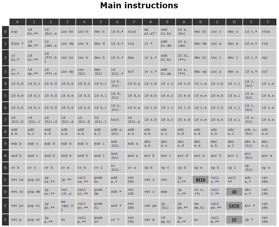
Figure 2: Z80 standard instruction set (source: clrhome.org)
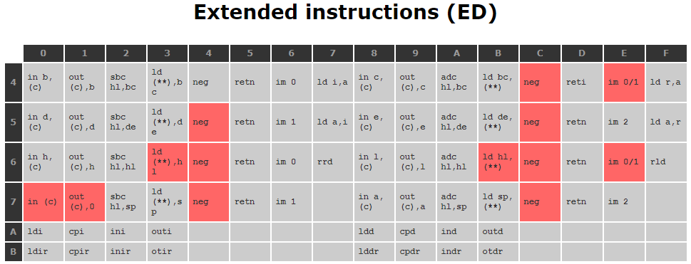
Figure 3: Z80 extended instruction set (source: clrhome.org)
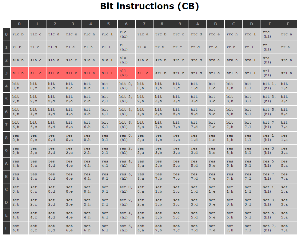
Figure 4: Z80 bit manipulation instruction (source: clrhome.org)
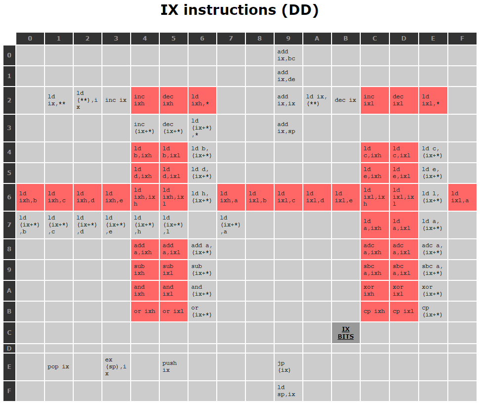
Figure 5: Z80 indexed (IX) instructions (source: clrhome.org)
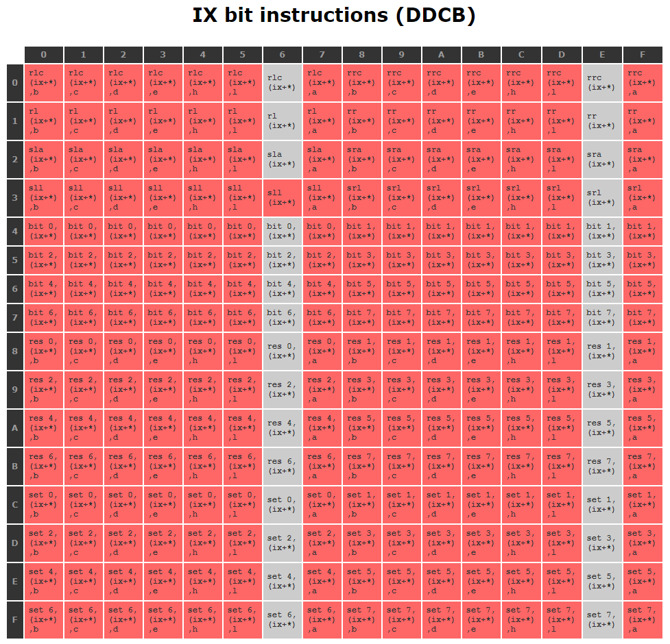
Figure 6: Z80 indexed (IX) bit manipulation operations (source: clrhome.org)
Timings
If you are about to write a ZX Spectrum emulator—or any computer emulator—you soon learn that taking care of timing is probably the most important thing. Without this, you won’t be able to create a high-fidelity emulation of real hardware.
Note: In the future articles in this series I will treat particular aspects of timings in almost every post.
The Z80 CPU executes instructions as a series of subsequent machine cycles. To understand how it works, Figure 7 gives you the detailed timing of the INC (HL) instruction. INC (HL) increments the value stored at the memory address pointed by the HL register pair.
As the figure shows, the CPU executes this instruction in four machine cycles:
- M1: The CPU reads the opcode from the memory address pointed by PC (Program Counter). The execution logic understands what this instruction means, and how to process it.
- M2: The CPU reads the contents of the memory address pointed by HL into some internal ALU register to be ready to process it.
- M3: The CPU increments the value of the internal ALU register
- M4: The CPU writes back the incremented value to the memory address pointed by HL.
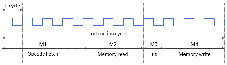
Figure 7: Timing diagram of the INC (HL) instruction
Well, this concise description of the M1…M4 cycles did not mention many subtle operation details. The real execution is more complicated. The diagram shows that the machine cycles utilize more than a single clock pulse (T-cycle) to carry out their tasks. The longest is M1 with four T-cycles. Reading and writing memory takes three T-cycles, respectively. The fastest step is the increment, it consumes a single clock cycle.
The M1 cycle is a special one, so I’d like to add some more details on it:
Every instruction starts with fetching the operation code. If the code is prefixed (such as in case of extended, indexed, and bit manipulation instructions), every opcode fetch is similar. The M1 cycle takes for T-cycles, T1, T2, T3, and T4. This is what happens during M1:
- As T1 begins, the CPU puts the contents of PC to the address bus. About a half T-cycle later, the CPU sign the MREQ (Memory Request) control signal in tandem with RD (Read).
- In T2, the memory responds by placing the content of the memory addressed by PC to the data bus. (By this time, the memory address stabilizes on the address bus.)
- Just as T3 begins, with the rising edge of the clock signal, the CPU reads the contents of the data bus—the opcode gets into one of the internal registers. The CPU revokes the RD, and MREQ signals and puts lower seven bit of R (Refresh Page Register) to the lower seven lines of the address bus. At the same time, the CPU places the contents of I (Interrupt Register), to the highest eight lines of the address bus, and signs RFSH (Refresh signal).
- During T3 and T4, when the refresh page address is stabilized on the address bus, the CPU raises the MREQ signal again. The combination of MREQ and RFSH allows the DRAM chips to refresh the memory contents of the addressed page.
- By the end of T3, the CPU analyzes the opcode read and prepares for the subsequent machine cycles. Many operations, are simple and do not need any further memory or I/O access. The CPU executes these operations during T4.
- By the end of T4, MREQ, RD (and RFSH, a little bit later) go back to their inactive state. The CPU increments the last seven bits of R while keeping its most significant bit.
As you can see, the M1 machine cycle is significant, it is responsible for refreshing the DRAM memory. Without this periodic refresh cycle, the memory would forget its content. Just to have an idea about this time, every page should be refreshed in every 64 milliseconds or less.
To let peripherals and other devices know that the CPU executes M1, Z80 has a system control signal, M1, that goes active during T1 and T2.
It may happen that during memory and I/O operations the CPU needs to wait while the memory or a device gets ready for a data transfer. The CPU has a WAIT input signal; devices may use it to sign that they are not prepared to let the CPU carry on the read or write operation.
Note: Later, in another post, you will learn that the $4000–$7FFF range of memory in ZX Spectrum 48K is contended. Sometimes, when the CPU wants to read or write the memory, it’s forced to WAIT, as the ULA has priority to keep the electron ray in the cathode tub uninterrupted.
Memory read and write, I/O read and write machine cycles have their detailed timings—similarly to M1. Here I won’t detail them. If you are interested, check the official Zilog Z80 documentation here.
Interrupts
The CPU cannot continuously poll devices whether they have something to tell. Devices can notify the CPU by generating an interrupt signal. Z80 receives that signal and suspends its normal execution. In response, it executes a routine, the interrupt routine. As that routine is completed, the CPU goes back and continues executing instructions right from the point it was before receiving the signal.
Z80 can handle two kinds of interrupts through the INT and NMI signals. NMI stands for Non-Maskable Interrupt. When the CPU receives an NMI request, it executes the interrupt routine starting at address $0066.
INT raises a maskable interrupt. Maskable means that you can disable (and re-enable) it from software—with the DI (Disable interrupt), and EI (Enable interrupt) Z80 instructions, respectively.
Z80 offers three interrupt handling modes. You can activate these with the IM 0, IM 1, and IM 2 instructions:
- IM 0: In this mode the interrupting device can force the CPU to execute a single machine operation. The device places the opcode to the address bus to let the CPU read it in. If the operation contains more bytes, the device should take care to provide those bytes according to the normal memory read timing sequence. No ZX Spectrum models use this interrupt mode.
- IM 1: This is the simplest interrupt mode. When the CPU receives the request, it starts the interrupt routine at address $0038. By default, all ZX Spectrum models—I mean, their operating system—uses this mode.
- IM 2: This mode is the most complex, often called vectored interrupt, for it allows an indirect call to any memory location by an 8-bit vector supplied from the peripheral device. This vector then becomes the least significant eight bits of the indirect pointer, while I (Interrupt Register) in the CPU provides the most significant eight bits. This address points to an address in a vector table that is the starting address for the interrupt service routine. ZX Spectrum games often use this mode to change the original interrupt handler routine entirely. Of course, the CPU cannot stash its current operation at the very moment an interrupt request arrives. Z80 defines an interrupt request/acknowledge timing cycle:
The CPU samples the INT signal with the rising edge of the final clock at the end of any instruction. The signal is not accepted unless the maskable interrupt is enabled. When the signal is accepted, the CPU generates a special M1 cycle. During this cycle, the IORQ signal becomes active (instead of the normal MREQ) to indicate that the interrupting device can place an 8-bit vector on the data bus. Two wait states are automatically added to this cycle. These states are added so that a ripple priority interrupt scheme can be easily implemented. The two wait states allow sufficient time for the ripple signals to stabilize and identify which I/O device must insert the response vector.
Next: Emulating the Z80A CPU
By now, you know enough information about the Z80 CPU. You are prepared to understand the operation of the Z80 emulator. In the next posts of this series, you will learn about the concepts, design, implementation, and testing details.