The zxnDMA: Moving Data Without the CPU
Somewhere around the third time you write a LDIR loop to fill screen memory, you start wondering: isn’t there a better way? The Z80’s block transfer instructions are fine for small jobs, but when you need to move kilobytes of data at full speed — loading sprite patterns, filling Layer 2 banks, streaming samples to the DAC — those 21 T-states per byte add up fast. At 3.5 MHz, copying a single 16KB memory bank with LDIR takes over 96 milliseconds. That’s nearly six frames of dead CPU time.
The ZX Spectrum Next has a built-in DMA controller that solves this problem. The zxnDMA — loosely based on the Zilog Z80 DMA chip but simplified and extended for the Next — can transfer data between any combination of memory and I/O ports, completely independently of the CPU. Think of it as a small moving company inside the FPGA: you give it the addresses, tell it how many boxes to shift, and it hauls bytes while the Z80 stops carrying furniture one byte at a time.
We’ll start with the concepts, work through the register structure, build up to practical transfer sequences, and finish with real-world patterns for sprite loading, memory filling, and audio streaming. Once the pattern clicks, a DMA transfer stops feeling like a ritual and starts looking like a compact little shipping order.
What this chapter assumes. You should already be comfortable with
OUT,OTIR, and port-based hardware from I/O Ports and NextRegs. The timed-transfer sections also lean on the CTC, and the sprite/audio examples make more sense once you’ve skimmed Sprites and DAC Audio.
What the DMA Actually Does
At its core, the DMA controller is a state machine that reads a byte from one place and writes it to another, over and over, until it’s done. “One place” and “another place” can each be a memory address or an I/O port. The DMA has its own address bus and data bus connections — when it’s active, the CPU steps aside (releases the bus) and the DMA takes over, reading and writing at hardware speed.
The process follows a simple cycle for each byte:
- Read from the source (memory or I/O port)
- Write to the destination (memory or I/O port)
- Update source and destination addresses (increment, decrement, or keep fixed)
- Count the byte and check if the transfer is complete
The DMA repeats this cycle for every byte in the block. A memory-to-memory transfer of 256 bytes takes roughly 256 × 6 T-states = 1,536 T-states at 3.5 MHz — about 440 microseconds. Compare that to LDIR’s 256 × 21 = 5,376 T-states. The DMA is roughly 3.5× faster for pure block copies, and the CPU no longer spends instructions moving the bytes itself.
There is a trade-off hiding in that last sentence. In continuous mode, the DMA owns the bus until the block finishes, so the CPU is paused during the transfer. In burst mode, the DMA gives the bus back between bytes or timed bursts, which lets the CPU keep doing useful work.
Two Ports, Two Personalities
The DMA controller is accessed through two I/O ports, and which port you use determines its operating mode:
| Port | Mode | Block Length Behavior |
|---|---|---|
0x6B | zxnDMA (Next-specific) | Transfers exactly N bytes |
0x0B | Z80 DMA (legacy Zilog compatible) | Transfers N + 1 bytes |
The difference is subtle but important. In legacy Z80 DMA mode, the byte counter starts at 0xFFFF (effectively −1) and counts up, so a block length of 0 transfers 1 byte, a block length of 1 transfers 2 bytes, and so on. In zxnDMA mode, the counter starts at 0 and a block length of N transfers exactly N bytes — which is what you’d expect. Unless you’re porting code from a system with a real Z80 DMA chip, always use port 0x6B.
Once you write to one port, the DMA “remembers” that mode until you write to the other port (which switches modes) or issue a hardware reset. In practice, most Next programs use
0x6Bexclusively and never think about it again.
The Port A / Port B Model
The DMA uses an unusual naming convention inherited from the Zilog Z80 DMA. Instead of “source” and “destination,” it has Port A and Port B. Each port can be configured independently as either a memory address or an I/O port, and can use different addressing modes (increment, decrement, or fixed).
A direction bit in the configuration determines which way data flows:
- A → B: Port A is the source, Port B is the destination
- B → A: Port B is the source, Port A is the destination
This flexibility means you can set up Port A as a memory pointer (incrementing through a buffer) and Port B as a fixed I/O address (always pointing at the same hardware register), then trigger a transfer that streams your buffer out to hardware. Or you can point both at memory addresses for a straightforward block copy.
The separation of “port identity” from “transfer direction” is a Zilog design choice rooted in the Z80 DMA’s history as a multi-purpose peripheral. It feels a little over-engineered for most Next use cases, but once you internalize the mental model, the programming sequence flows naturally.
Three Ways to Write a DMA Program
All DMA configuration amounts to bytes arriving at the DMA port. The hardware doesn’t care how those bytes were produced — from individual OUT (C),A instructions, from an OTIR loop reading a byte table, or from a Klive assembler .dma pragma. All three approaches produce identical binary output. What changes is readability, maintainability, and which assembler you’re using.
Style 1: Direct OUT Instructions
The most explicit approach writes each configuration byte with a LD A,value : OUT (C),A pair. The register-documentation sections later in this chapter use this style because it maps one-to-one onto the bit-field diagrams:
    ld bc,$6B
    ld a,$C3               ; WR6: Reset
    out (c),a
    ld a,$7D               ; WR0: A→B, transfer, all follow-bytes set
    out (c),a
    ld a,$00               ; Port A low byte (0x8000)
    out (c),a
    ; ...
When to use it: Fully runtime-dynamic values — addresses in registers, lengths computed on the fly. Every byte can be a live register value; each OUT carries whatever A happens to hold.
Constraints: Verbose — a complete sequence is 15–20 paired LD / OUT instructions. The raw hex values ($7D, $2D, $28…) carry no self-documentation; you need the register bit-field diagrams beside you to read the code.
Style 2: The OTIR Table Pattern
Store the entire DMA program as a contiguous byte table in RAM. Label any fields that need runtime patching, patch those fields before the upload, then stream the whole table to the DMA port with a single OTIR:
    ; Patch the two dynamic fields
    ld (dmaSrc),hl             ; source address (computed at runtime)
    ld (dmaLen),bc             ; byte count     (computed at runtime)

    ; Upload — five instructions, regardless of program length
    ld hl,dmaProgram
    ld b,dmaProgram_end - dmaProgram
    ld c,$6B
    otir
    ret

dmaProgram:
    .db $C3                     ; WR6: Reset
    .db $7D                     ; WR0: all params, A→B, transfer
dmaSrc:
    .dw 0                       ; Port A address — patched at runtime
dmaLen:
    .dw 0                       ; Block length   — patched at runtime
    .db $14                     ; WR1: memory, increment
    .db $10                     ; WR2: memory, increment
    .db $2D                     ; WR4: continuous, Port B address follows
    .dw $C000                   ; Port B address — constant
    .db $CF                     ; WR6: Load
    .db $87                     ; WR6: Enable
dmaProgram_end:
When to use it: Semi-static programs where most configuration is fixed at assembly time and only a small number of fields (typically source address and block length) need runtime patching. This pattern is widely used in community examples and references for the ZX Spectrum Next.
Constraints: The table must live in RAM, not ROM — LD (label),HL patching requires writable memory. The raw hex bytes in the table body are just as opaque as Style 1: $7D still doesn’t tell you it means “A→B, transfer, all follow-bytes set.”
A note on OTIR and the port address: OTIR outputs to port (C) and decrements B after each byte, so by the time the last byte is sent, B has counted down to zero. Because the Z80’s OUT (C),A instruction puts the full 16-bit BC register on the address bus, the upper byte of the port address changes with every iteration. This sounds alarming, but it is harmless here: the zxnDMA port decoder looks only at the lower 8 bits of the address bus ($6B) and ignores the upper 8 bits entirely. Every byte in the table therefore lands at the correct port regardless of what B holds at that moment.
Compatibility: Works with any Z80 assembler — sjasmplus, Pasmo, or any other tool that supports DB/DW directives. No assembler extensions required.
Style 3: The .dma Pragma (Klive Assembler)
The Klive Z80 Assembler’s .dma pragma emits exactly the same byte sequences as a hand-crafted DB/DW table, but replaces raw hex encodings with named sub-commands and parameter keywords:
dmaProgram:
    .dma reset
    .dma wr0 a_to_b, transfer       ; base byte only — address and length follow
dmaSrc:
    .dw 0                           ; Port A address — patched at runtime
dmaLen:
    .dw 0                           ; Block length   — patched at runtime
    .dma wr1 memory, increment
    .dma wr2 memory, increment
    .dma wr4 continuous             ; base byte only — Port B address follows
    .dw $C000                       ; Port B address — constant
    .dma wr5
    .dma load
    .dma enable
dmaProgram_end:
The upload is identical to Style 2 — a five-instruction OTIR sequence:
    ld (dmaSrc),hl
    ld (dmaLen),bc
    ld hl,dmaProgram
    ld b,dmaProgram_end - dmaProgram
    ld c,$6B
    otir
When to use it: Any time you’re using the Klive assembler and want readable, self-documenting DMA code — which is almost always. The emitted bytes are bit-for-bit identical to the hand-crafted DB table, so there is zero runtime overhead.
Constraints:
- Klive assembler only. Not compatible with sjasmplus, Pasmo, or other tools.
- Compile-time constants only. Sub-command parameters (e.g.
wr0 a_to_b, transfer, $8000, 256) must be resolvable at assembly time. For runtime addresses, omit the optional parameter and patch a.dw 0label as shown above. - Follow-byte indicator bits are always set.
WR0andWR4base bytes always have all address/length follow-byte indicator bits set regardless of whether you supply the optional parameters. This is correct — it means the.dwpatch labels that follow are consumed as the expected follow bytes.
Which Style This Chapter Uses
The register-documentation sections (WR0 through WR6) use Style 1 — direct OUT instructions — because the byte-at-a-time structure maps naturally onto the bit-field diagrams.
All practical patterns and complete examples use Style 3 — the .dma pragma combined with the OTIR upload sequence. The labels over .dw 0 patch points are self-documenting, and the pragma sub-command names make register configuration immediately readable.
If you’re working with a different assembler, translate any .dma pragma block to an equivalent DB/DW table and upload with OTIR — the byte sequences are identical.
Programming the DMA: Register Groups
All DMA configuration happens by writing sequences of bytes to either port 0x6B or 0x0B. There’s no separate register select mechanism — the DMA determines which register you’re programming based on bit patterns in the first byte (the “base byte”) of each write sequence.
The DMA has seven register groups, WR0 through WR6:
| Register | Purpose | Key Configurations |
|---|---|---|
| WR0 | Transfer direction, Port A address, block length | Direction (A→B or B→A), source address, transfer size |
| WR1 | Port A configuration | Memory vs I/O, address mode, timing |
| WR2 | Port B configuration | Memory vs I/O, address mode, timing, prescaler |
| WR3 | Interrupt and match control | Enable/disable, mask and match bytes |
| WR4 | Operating mode, Port B address | Continuous/Burst mode, destination address |
| WR5 | Control flags | Auto-restart, CE/WAIT behavior |
| WR6 | Commands | Reset, Load, Enable, Disable, Read Status |
How the Base Byte Dispatch Works
Each register group has a unique bit pattern in its base byte that the DMA uses for identification. The detection follows a priority order — the first match wins:
D7=0, D2:D0 = 000  → WR2  (Port B configuration)
D7=0, D2:D0 = 100  → WR1  (Port A configuration)
D7=0                → WR0  (catch-all for D7=0: direction, addresses, block length)
D7=1, D1:D0 = 00   → WR3  (Interrupt/match control)
D7=1, D1:D0 = 01   → WR4  (Operating mode, Port B address)
D7:D6=10, D2:D0=010 → WR5 (Control flags)
else                → WR6  (Commands)
This means you cannot write arbitrary bytes and hope the DMA guesses your intent. Each configuration byte must have the correct bit pattern for the register you’re targeting. The diagrams in the next sections show the exact encoding for each register.
Follow Bytes
Most register groups use a “follow byte” mechanism: control bits in the base byte indicate whether additional parameter bytes will follow. For example, WR0’s base byte has bits that say “Port A address low byte follows,” “Port A address high byte follows,” “block length low byte follows,” and “block length high byte follows.” The DMA expects those follow bytes in order, immediately after the base byte.
This means a WR0 write with all parameters is five bytes: the base byte plus four follow bytes (two for the address, two for the block length). If you only need to change the direction without updating addresses, you write just the base byte with the follow bits cleared — no extra bytes needed.
WR0: Direction, Port A Address, and Block Length
WR0 configures the transfer direction, sets Port A’s starting address, and specifies how many bytes to transfer. It’s almost always the first register you program in a transfer sequence.
Base byte format:
Bit 7: 0 (identifies this as WR0/WR1/WR2 group)
Bit 6: 1 = block length high byte follows
Bit 5: 1 = block length low byte follows
Bit 4: 1 = Port A address high byte follows
Bit 3: 1 = Port A address low byte follows
Bit 2: Direction — 1 = A→B, 0 = B→A
Bit 1-0: Transfer type — 01 = Transfer, 10 = Search, 11 = Search+Transfer
When you want a standard memory-to-memory or memory-to-I/O transfer with all parameters, the base byte is 0x7D:
- D6=1, D5=1 (block length follows, both bytes)
- D4=1, D3=1 (Port A address follows, both bytes)
- D2=1 (A→B direction)
- D1=0, D0=1 (Transfer mode)
Follow bytes (when indicated by base byte bits):
- Port A address, low byte
- Port A address, high byte
- Block length, low byte
- Block length, high byte
Here’s a complete WR0 write that sets up a 256-byte transfer from address 0x8000, direction A→B:
    ld bc,$6B          ; DMA port (zxnDMA mode)
    ld a,$7D           ; WR0: all params follow, A→B, Transfer mode
    out (c),a
    ld a,$00           ; Port A address low = 0x00
    out (c),a
    ld a,$80           ; Port A address high = 0x80
    out (c),a
    ld a,$00           ; Block length low = 0x00 (256 & 0xFF)
    out (c),a
    ld a,$01           ; Block length high = 0x01 (256 >> 8)
    out (c),a
Block length encoding: The block length is a 16-bit value. A length of 256 is written as
0x0100(low byte0x00, high byte0x01). In zxnDMA mode, this transfers exactly 256 bytes. Be careful not to confuse a block length of 0 with “nothing to transfer” — depending on the mode and DMA state, it can behave unexpectedly.
WR1: Port A Configuration
WR1 tells the DMA how Port A behaves: whether it points to memory or an I/O port, and what happens to the address after each byte.
Base byte format:
Bit 7: 0
Bit 6: 1 = timing byte follows
Bit 5-4: Address mode — 00 = Decrement, 01 = Increment, 10/11 = Fixed
Bit 3: Port type — 1 = I/O port, 0 = Memory
Bit 2-0: 100 (WR1 identifier)
For a typical memory source with incrementing addresses, the base byte is 0x14:
- D6=0 (no timing byte)
- D5:D4=01 (increment after each byte)
- D3=0 (memory, not I/O)
- D2:D0=100 (WR1 identifier)
    ld a,$14           ; WR1: memory, increment, no timing byte
    out (c),a
Address Modes Explained
The address mode controls what happens to the port’s address after each byte transfer:
| D5:D4 | Mode | Behavior |
|---|---|---|
| 00 | Decrement | Address decreases by 1 after each byte |
| 01 | Increment | Address increases by 1 after each byte |
| 10 | Fixed | Address stays the same for every byte |
| 11 | Fixed | Same as 10 — address doesn’t change |
Increment mode is by far the most common — it’s what you use for block copies, loading sprite data, filling memory. Fixed mode is essential when one end of the transfer is an I/O port: you want the port address to stay the same while the memory address walks through the buffer.
Decrement mode is useful for overlapping copies where the destination overlaps the source from below — the same reason you’d choose LDDR over LDIR in standard Z80 code.
Timing Configuration
If bit 6 of the base byte is set, a timing byte follows:
Timing byte:
Bit 5: 1 = prescaler byte follows (WR2 only — ignored in WR1)
Bit 1-0: Cycle length — 00 = 4 T-states, 01 = 3 T-states, 10 = 2 T-states
Most transfers work fine with the default 3-T-state timing. You’d only change this for specialized scenarios like matching a peripheral’s timing requirements.
WR2: Port B Configuration
WR2 is the mirror of WR1 but for Port B, with one important addition: it can configure a prescaler for paced burst transfers (used primarily for audio streaming).
Base byte format:
Bit 7: 0
Bit 6: 1 = timing byte follows
Bit 5-4: Address mode — 00 = Decrement, 01 = Increment, 10/11 = Fixed
Bit 3: Port type — 1 = I/O port, 0 = Memory
Bit 2-0: 000 (WR2 identifier)
For a memory destination with incrementing addresses: 0x10 (same structure as WR1 but with 000 in D2:D0).
The Prescaler
The prescaler is a ZXN DMA extension that doesn’t exist in the original Zilog Z80 DMA. In burst-style transfers, it inserts a precise delay between bytes, which lets you stream data at a controlled rate — perfect for digital audio playback. Do not use it as a way to slow down an ordinary continuous memory copy; on current hardware, continuous memory transfers use their normal DMA cycle timing.
To set a prescaler:
- Set bit 6 in WR2’s base byte (timing byte follows)
- Write the timing byte with bit 5 set (prescaler follows)
- Write the prescaler value
The delay formula is:
T-states per byte = (prescaler * 3,500,000) / 875,000
                  = prescaler * 4
So a prescaler value of 80 gives 320 T-states between transfers — about 91 microseconds at 3.5 MHz, which corresponds to a sample rate of roughly 10.9 kHz. A prescaler of 20 gives 80 T-states (approximately 43.75 kHz, close to CD quality at 44.1 kHz).
The internal FPGA implementation uses a 14-bit timer that counts at different rates depending on the CPU speed:
| CPU Speed | Timer Increment per Clock |
|---|---|
| 3.5 MHz | 8 |
| 7 MHz | 4 |
| 14 MHz | 2 |
| 28 MHz | 1 |
The DMA compares the prescaler value against DMA_timer[13:5] — the upper 9 bits of this 14-bit counter — to decide when the next byte can transfer. This scaling ensures the prescaler produces the same real-time delay regardless of the CPU speed setting.
    ; WR2 with prescaler for audio streaming
    ld a,$60           ; WR2: timing follows, increment, memory
    out (c),a
    ld a,$22           ; Timing: prescaler follows (D5=1), 2 T-state cycles (D1:D0=10)
    out (c),a
    ld a,80            ; Prescaler value = 80 (→ 320 T-states between transfers)
    out (c),a
WR3: Interrupt and Match Control
WR3 handles interrupt generation and search matching. The FPGA implementation comments out most of the search/match logic (it’s not fully supported in hardware), but the basic enable and interrupt control bits work.
Base byte format:
Bit 7: 1
Bit 6: 1 = Enable DMA (via WR3 — older method, prefer WR6 command 0x87)
Bit 5: Interrupt enable
Bit 4: 1 = match byte follows
Bit 3: 1 = mask byte follows
Bit 2: Stop on match
Bit 1-0: 00 (WR3 identifier)
In practice, most programs control the DMA exclusively through WR6 commands and don’t touch WR3 directly. The exception is when you need the search functionality (finding a specific byte value during a transfer) or when setting up interrupts.
Search Mode
When WR0’s transfer type is set to Search (D1=1) or Search+Transfer (D1=1, D0=1), the DMA compares each byte read against a match pattern with a mask:
Match condition: (readByte | MASK) == (MATCH | MASK)Bits set to 1 in the mask are “don’t care” — they’re forced to 1 in both the read byte and the match byte before comparison. A mask of 0x00 requires an exact match; a mask of 0xFF matches everything.
When a match is found:
- A status bit is set
- If interrupt-on-match is enabled, an interrupt fires
- If stop-on-match is set (WR5 D2), the transfer halts
In pure Search mode (WR0 D0=0), the DMA reads bytes and checks for matches without writing them anywhere. In Search+Transfer mode (D1=1, D0=1), it transfers the byte and checks for a match.
WR4: Operating Mode and Port B Address
WR4 sets the transfer mode and provides Port B’s starting address.
Base byte format:
Bit 7: 1
Bit 6-5: Operating mode — 00 = Byte, 01 = Continuous, 10 = Burst
Bit 4: 1 = interrupt control byte follows
Bit 3: 1 = Port B address high byte follows
Bit 2: 1 = Port B address low byte follows
Bit 1-0: 01 (WR4 identifier)
Follow bytes:
- Port B address, low byte (if D2=1)
- Port B address, high byte (if D3=1)
- Interrupt control byte (if D4=1) — not implemented in the Next FPGA
Operating Modes
The operating mode determines how the DMA interacts with the CPU bus:
Continuous mode (D6:D5 = 01): The DMA grabs the bus once and holds it until the entire block is transferred. This is the fastest mode — the CPU is completely halted for the duration. For a 256-byte memory-to-memory copy, that’s about 1,536 T-states of CPU downtime. The advantage is that no bus arbitration overhead is wasted between bytes.
Burst mode (D6:D5 = 10): The DMA can release and re-request the bus between groups of bytes. When combined with the prescaler, burst mode allows the CPU to run between timed transfers — essential for audio playback where you need to stream bytes at a fixed rate while the CPU handles other tasks. In burst mode, the DMA releases the bus during prescaler wait periods, giving the CPU those cycles back.
Byte mode (D6:D5 = 00): Transfers one byte per bus grant. Not commonly used on the Next — continuous mode handles most needs, and burst mode with a prescaler handles the rest.
For most transfers, you’ll use continuous mode. Audio streaming uses burst mode with a prescaler.
    ; WR4: Continuous mode, Port B address follows
    ld a,$2D           ; D6:D5=01 (continuous), D3=1 (addr hi), D2=1 (addr lo), D1:D0=01
    out (c),a
    ld a,$00           ; Port B address low
    out (c),a
    ld a,$C0           ; Port B address high (i.e., 0xC000)
    out (c),a
WR5: Control Flags
WR5 is a simple single-byte register with control flags.
Base byte format:
Bit 7-6: 10
Bit 5: Auto-restart — 1 = reload addresses and restart on block completion
Bit 4: CE/WAIT multiplexed
Bit 3: Ready active high (not used on Next)
Bit 2-0: 010 (WR5 identifier)
Auto-Restart
When auto-restart is enabled, the DMA automatically reloads Port A and Port B starting addresses and the block length counter when a transfer completes, then starts a new transfer immediately. This creates an endless loop of transfers — useful for repeated patterns or continuous streaming.
The FPGA implements auto-restart in the FINISH_DMA state: it copies the registered start addresses back into the working source and destination pointers, resets the byte counter, and jumps back to the start of the transfer sequence.
    ld a,$A2           ; WR5: auto-restart enabled (D5=1)
    out (c),a
WR6: Command Register
WR6 is the command register — it doesn’t configure anything persistently; instead, it triggers immediate actions. This is where the real control happens.
Key commands:
| Command | Hex | What it does |
|---|---|---|
| Reset | 0xC3 | Full DMA reset — clears all registers and state |
| Reset Port A Timing | 0xC7 | Reset Port A timing to defaults (3 T-state cycles) |
| Reset Port B Timing | 0xCB | Reset Port B timing to defaults |
| Disable DMA | 0x83 | Stop any active transfer |
| Load | 0xCF | Load start addresses into transfer engine |
| Continue | 0xD3 | Reset byte counter, keep current addresses |
| Enable DMA | 0x87 | Start the transfer |
| Read Status Byte | 0xBF | Prepare status for reading |
| Initialize Read Sequence | 0xA7 | Set up multi-register read sequence |
| Reinitialize Status Byte | 0x8B | Clear status flags |
| Read Mask Follows | 0xBB | Next byte sets which registers appear in read sequence |
| Force Ready | 0xB3 | Force ready signal (for testing) |
| Enable Interrupts | 0xAB | Set interrupt enable bit |
| Disable Interrupts | 0xAF | Clear interrupt enable bit |
The three commands you’ll use in virtually every transfer are Reset, Load, and Enable DMA.
The LOAD Command — a Common Gotcha
A frequent mistake is to configure all the registers and then call Enable DMA without calling Load first. The Load command (0xCF) copies the addresses from WR0 and WR4 into the DMA’s internal transfer engine. Without Load, the DMA starts transferring from whatever addresses happen to be left over from the previous transfer — or from zero if this is the first use.
The Load command also:
- Initializes the byte counter (0 in zxnDMA mode, 0xFFFF in legacy mode)
- Sets up the direction (copies Port A to source and Port B to destination, or vice versa, based on WR0’s direction bit)
- Clears the end-of-block status
Always call Load after configuring addresses and before calling Enable.
Progressive Reset
Here’s something that surprises most programmers: the Reset command (0xC3) uses a progressive reset mechanism. Each call clears one column of the register array, and it takes six consecutive Reset calls to fully clear every register. This matches the original Zilog Z80 DMA behavior.
In practice, one Reset is usually enough — it stops any active transfer, clears the DMA state machine, resets timing to defaults, and puts the DMA in a known idle state. The progressive column clearing means some register fields might retain old values, but since you’re about to reprogram everything anyway, it rarely matters.
Reading DMA Status
You can read the DMA’s current state by reading from the same port you write to (0x6B or 0x0B). The status byte format is:
Bit 5: End of block (inverted: 1 = not reached, 0 = reached)
Bit 4: Constant 1
Bit 3: Constant 1
Bit 2: Constant 0
Bit 1: Constant 1
Bit 0: At least one byte transferred (1 = yes)

Format: 00E11010 or 00E11011
To read the status byte alone, write the Read Status Byte command (0xBF) and then read from the port:
    ld bc,$6B
    ld a,$BF           ; Read Status Byte command
    out (c),a
    in a,(c)           ; Read status
    bit 5,a            ; Test end-of-block flag
    jr z,.transferDone ; If bit 5 = 0, transfer is complete
Extended Read Sequence
For more detailed monitoring, the DMA supports reading multiple internal registers in sequence. Use the Read Mask Follows command (0xBB) followed by a mask byte to select which registers to include:
| Mask Bit | Register |
|---|---|
| Bit 0 | Status byte |
| Bit 1 | Byte counter, low |
| Bit 2 | Byte counter, high |
| Bit 3 | Port A address, low |
| Bit 4 | Port A address, high |
| Bit 5 | Port B address, low |
| Bit 6 | Port B address, high |
After setting the mask and issuing the Initialize Read Sequence command (0xA7), each read from the port returns the next enabled register in order, cycling through the enabled set.
    ld bc,$6B
    ld a,$BB           ; Read mask follows
    out (c),a
    ld a,$07           ; Mask: status + counter lo + counter hi
    out (c),a
    ld a,$A7           ; Initialize read sequence
    out (c),a
    in a,(c)           ; → status byte
    in a,(c)           ; → byte counter low
    in a,(c)           ; → byte counter high
Putting It All Together: The Standard Transfer Sequence
Every DMA transfer follows the same pattern. Once you’ve seen it a few times, it becomes second nature:
- Reset the DMA to a known state
- Configure WR0 (direction, Port A address, block length)
- Configure WR1 (Port A: memory/IO, address mode)
- Configure WR2 (Port B: memory/IO, address mode)
- Configure WR4 (operating mode, Port B address)
- Load addresses into the transfer engine
- Enable the DMA
Let’s build a complete example: copying 256 bytes from address 0x8000 to 0xC000, using the .dma pragma with the OTIR upload pattern:
dmaCopyProgram:
    .dma reset
    .dma wr0 a_to_b, transfer, $8000, 256   ; Step 2: direction, Port A, block length
    .dma wr1 memory, increment              ; Step 3: Port A — memory, incrementing
    .dma wr2 memory, increment              ; Step 4: Port B — memory, incrementing
    .dma wr4 continuous, $C000              ; Step 5: continuous mode, Port B = 0xC000
    .dma wr5                                ; Step 5 cont.: control flags (defaults)
    .dma load                               ; Step 6: load addresses into transfer engine
    .dma enable                             ; Step 7: start the transfer
dmaCopyProgram_end:

DmaCopy:
    ld hl,dmaCopyProgram
    ld b,dmaCopyProgram_end - dmaCopyProgram
    ld c,$6B
    otir
    ret
The OTIR upload is five instructions regardless of how many configuration bytes the program contains. The .dma pragma sub-command names annotate each step inline — a_to_b, transfer, $8000, 256 is self-explanatory where the equivalent raw bytes ($7D $00 $80 $00 $01) are not. The DMA will execute the 256-byte copy in about 1,536 T-states — during which the CPU is halted — and then release the bus.
You can find a demonstration of using the DMA for copying in the DmaDemo.SimpleMemCopy example.
Demo: Comparing LDIR and zxnDMA
Let’s put numbers on the feeling. This demo copies the same 2 KB screen-memory block twice: first with LDIR, then with zxnDMA. Both measurements use the CTC timing helper from Chapter 5: Timing.SetupCtc16, Timing.StartMeasure, and Timing.GetMeasuredCounter.
The block lives in the ULA pixel area, so the demo does not reserve a large private source and two large destination buffers. It uses $4000..$47FF as the source, $4800..$4FFF as the LDIR destination, and $5000..$57FF as the DMA destination. Because those addresses are visible screen memory, the demo measures first, clears the pixel area, and only then prints the results.
.module DmaCompareDemo

DMA_PORT  .equ $6b
COPY_SIZE .equ $0800       ; 2048 bytes
SRC_ADDR  .equ $4000
LDIR_DEST .equ $4800
DMA_DEST  .equ $5000

;==========================================================
; Compare LDIR and zxnDMA for the same 2 KB memory copy
;==========================================================
LdirAndDma
    ; Fill the source screen area with a visible pattern.
    ld hl,SRC_ADDR
    ld bc,COPY_SIZE
`fillSource
    ld (hl),$aa
    inc hl
    dec bc
    ld a,b
    or c
    jr nz,`fillSource

    ; --- Measure the LDIR version
    call Timing.SetupCtc16
    call Timing.StartMeasure

    ld hl,SRC_ADDR
    ld de,LDIR_DEST
    ld bc,COPY_SIZE
    ldir

    call Timing.GetMeasuredCounter
    ld (@LdirTicks),de

    ; Prepare the DMA transfer before starting the stopwatch.
    ; The program ends with LOAD, but not ENABLE.
    ld hl,@DmaCopyProgram
    ld b,@DmaCopyProgramEnd - @DmaCopyProgram
    ld c,DMA_PORT
    otir

    ; --- Measure the DMA version
    call Timing.SetupCtc16
    call Timing.StartMeasure

    ld bc,DMA_PORT
    ld a,$87                ; WR6: Enable DMA
    out (c),a

`waitDma
    ld bc,DMA_PORT
    ld a,$bf                ; WR6: Read Status Byte
    out (c),a
    in a,(c)
    bit 5,a                 ; 0 = end of block reached
    jr nz,`waitDma

    call Timing.GetMeasuredCounter
    ld (@DmaTicks),de

    ; The benchmark used visible screen memory as scratch space.
    ; Clear it before printing the result.
    call @ClearPixels
    Display.PrintTitle(@Title)
    Display.PrintText(@Instr)

    ; --- Show both tick counts
    Display.PrintAt(8,0)
    Display.Ink(Color.Black)
    Display.PrintText(@TextLdir)
    ld hl,(@LdirTicks)
    Display.Ink(Color.Blue)
    Display.PrintHLDecimal()

    Display.PrintAt(9,0)
    Display.Ink(Color.Black)
    Display.PrintText(@TextDma)
    ld hl,(@DmaTicks)
    Display.Ink(Color.Blue)
    Display.PrintHLDecimal()
    ret

;----------------------------------------------------------
; Clear the 6144-byte ULA pixel area without using DMA.
; We want the screen tidy before displaying the measured values.
;----------------------------------------------------------
@ClearPixels
    ld hl,$4000
    ld de,$4001
    ld bc,6143
    xor a
    ld (hl),a
    ldir
    ret

@DmaCopyProgram
    .dma reset
    .dma wr0 a_to_b, transfer, SRC_ADDR, COPY_SIZE
    .dma wr1 memory, increment
    .dma wr2 memory, increment
    .dma wr4 continuous, DMA_DEST
    .dma wr5
    .dma load
@DmaCopyProgramEnd

@LdirTicks
    .defw 0

@DmaTicks
    .defw 0

@Title
    .defn "DMA #2: LDIR vs zxnDMA"

@Instr
    .defm "Copies the same 2 KB screen\x0d"
    .defm "block twice: LDIR, then DMA.\x0d"
    .defm "The values are CTC ticks from\x0d"
    .defn "Chapter 5's timing helper.\x0d\x0d"

@TextLdir
    .defn "LDIR ticks: "

@TextDma
    .defn "DMA ticks:  "

.endmoduleTry the DmaCompareDemo.LdirAndDma example.
The DMA program is uploaded before the stopwatch starts and deliberately ends with .dma load, not .dma enable. The timed block sends the Enable DMA command and then polls the DMA status byte until the end-of-block flag says the transfer has finished. That status wait is the timing boundary: without it, you mostly measure the command that starts DMA, not the copy.
This keeps the OTIR program upload out of the measurement while still waiting for the actual transfer to complete. In real code you still pay the setup cost somewhere, but you can often reuse a prepared DMA table and only patch the fields that change.
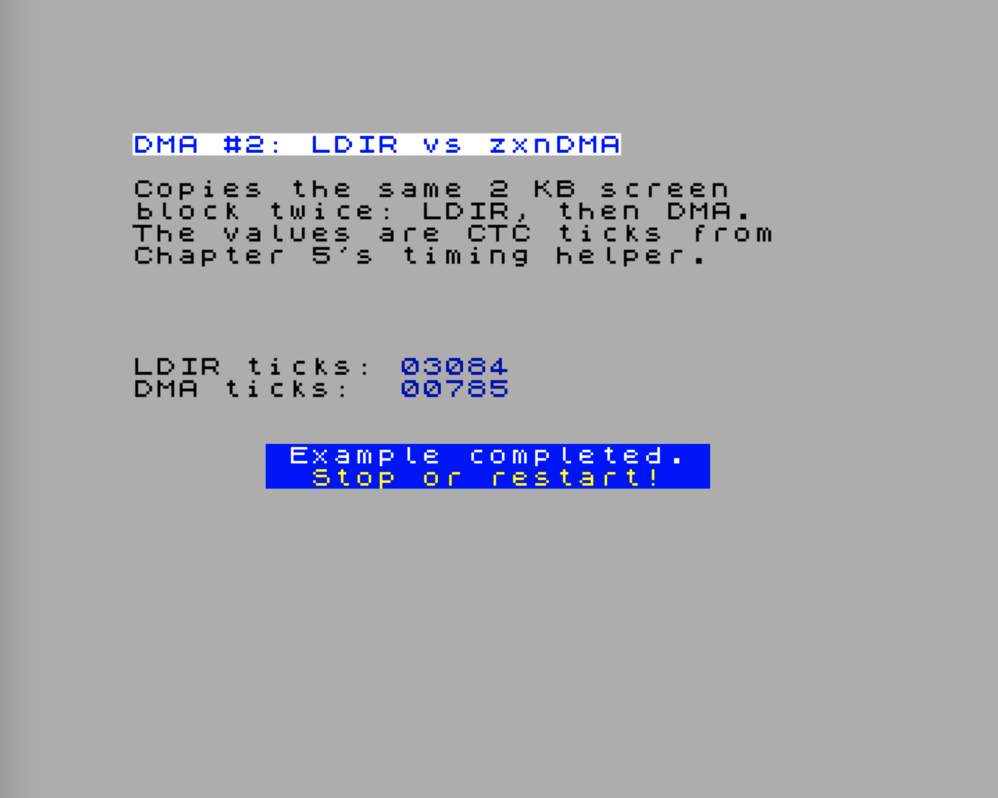
The raw values are CTC ticks, not microseconds. As the figure indicates, the DMA transfer is significantly faster (~ four times) than the LDIR copy. With the nominal Chapter 5 timing setup, one tick is about 571 ns, so you can convert a result with:
microseconds ≈ ticks × 0.571The timing helper counts 28 MHz clock time in groups of 16 clocks. That makes the DMA result easy to predict. With the default .dma wr1 memory, increment and .dma wr2 memory, increment settings, the Next’s DMA engine uses a 3-clock memory read followed by a 3-clock memory write. A 2 KB copy therefore needs:
2048 bytes × 6 clocks/byte = 12288 clocks
12288 clocks / 16 clocks per CTC tick = 768 ticks
The value printed by the demo is usually a little higher than 768 ticks, because the measured block also includes the Enable DMA port write and the final status polling loop. A result around 780-790 ticks is exactly the kind of number you should expect at 28 MHz.
LDIR is different. Each repeated byte copy takes 21 CPU T-states before any Next-specific memory effects are considered:
2048 bytes × 21 T-states/byte = 43008 T-states
43008 / 16 = 2688 CTC ticks
The visible result is higher than that simple 2688-tick baseline because this benchmark reads from and writes to the ULA pixel area. Screen memory is not just ordinary scratch RAM: display contention and the 28 MHz memory schedule can stretch CPU memory accesses. So a value around 3000 ticks for LDIR is plausible for this particular screen-memory copy.
Do not expect this visible-screen benchmark to show a clean abstract speedup from the instruction tables alone. The source and both destinations live in the ULA pixel area, so video contention and 28 MHz memory timing are part of the measurement. That is intentional: this demo keeps the scratch space out of your program body while still showing why DMA is the better tool for block movement.
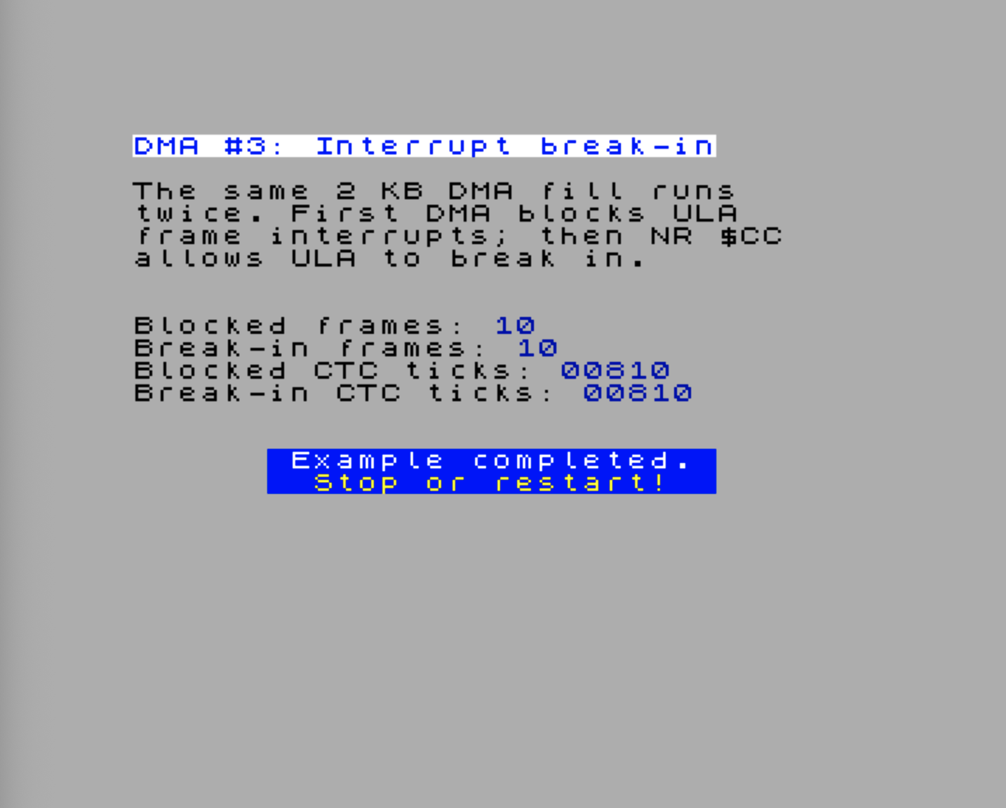
Demo: Letting Interrupts Break Into a Long DMA Transfer
Continuous DMA is fast, but it normally owns the bus until the block finishes. That means the CPU cannot run ordinary interrupt handlers while the transfer is in progress. The Next gives you a second set of interrupt-enable registers, $CC–$CE, that control which interrupt sources may ask the DMA to pause and give the bus back temporarily.
This demo runs the same continuous DMA fill twice. A ULA frame ISR toggles the border and increments a counter. In the first pass, DMA runs as one uninterrupted block; interrupts remain disabled while the stopwatch is running so the timing does not accidentally include a ULA frame ISR that was latched during the transfer. In the second pass, NR $CC bit 0 is set, so the ULA frame interrupt is allowed to interrupt the DMA. The fill destination is $5000, in the lower third of the ULA bitmap, so the title and instruction text at the top of the screen stay readable.
.module DmaInterruptDemo

DMA_PORT        .equ $6b

NR_INT_CONTROL  .equ $c0
NR_INT_EN_0     .equ $c4
NR_INT_STATUS_0 .equ $c8
NR_DMA_INT_EN_0 .equ $cc

VECTOR_TOP_BITS .equ %01100000
ULA_PRIORITY    .equ 11
ULA_VECTOR      .equ VECTOR_TOP_BITS | (ULA_PRIORITY << 1)

DMA_DEST        .equ $5000
DMA_FILL_SIZE   .equ $0800       ; 2048 bytes
ISR_CTC_COST    .equ 12          ; Approximate ULA ISR cost in CTC ticks

;==========================================================
; DMA interrupt break-in demo
;==========================================================
DmaInterruptBreakIn
    Display.PrintTitle(@Title)
    Display.PrintText(@Instr)

    di
    call Timing.SetupCtc16

    ; --- Set up hardware IM2 for the ULA frame interrupt.
    ld a,high(@VectorTable)
    ld i,a
    im 2
    nextreg NR_INT_CONTROL,VECTOR_TOP_BITS | $01
    nextreg NR_INT_EN_0,%00000001        ; CPU may receive ULA frame INTs
    nextreg NR_INT_STATUS_0,%00000001

    ; --- Pass 1: DMA runs as one uninterrupted block.
    ;     Keep IFF disabled so the CTC measurement does not include
    ;     a frame ISR that was latched while DMA owned the bus.
    xor a
    ld (@FrameTicks),a
    ld (@BorderColour),a
    nextreg NR_DMA_INT_EN_0,%00000000    ; ULA may not interrupt DMA
    nextreg NR_INT_STATUS_0,%00000001
    call Timing.StartMeasure

    call @RunDmaFill

    ld a,(@FrameTicks)
    ld (@BlockedTicks),a
    call Timing.GetMeasuredCounter
    ld (@BlockedDmaTicks),de

    ; --- Pass 2: allow the ULA frame interrupt to break into DMA.
    xor a
    ld (@FrameTicks),a
    ld (@BorderColour),a
    nextreg NR_INT_STATUS_0,%00000001
    nextreg NR_DMA_INT_EN_0,%00000001    ; bit 0 mirrors ULA for DMA
    call Timing.StartMeasure
    ei

    call @RunDmaFill

    ld a,(@FrameTicks)
    ld (@BreakInTicks),a
    call Timing.GetMeasuredCounter
    ld a,(@BreakInTicks)
    call @SubtractIsrCost
    ld (@BreakInDmaTicks),de

    ; --- Restore the normal interrupt setup.
    nextreg NR_DMA_INT_EN_0,0
    nextreg NR_INT_STATUS_0,%00000001
    nextreg NR_INT_CONTROL,0
    im 1
    ei

    ; --- Show the two counters.
    Display.PrintAt(8,0)
    Display.Ink(Color.Black)
    Display.PrintText(@TextBlocked)
    ld a,(@BlockedTicks)
    Display.Ink(Color.Blue)
    Display.PrintAHexadecimal()

    Display.PrintAt(9,0)
    Display.Ink(Color.Black)
    Display.PrintText(@TextBreakIn)
    ld a,(@BreakInTicks)
    Display.Ink(Color.Blue)
    Display.PrintAHexadecimal()

    Display.PrintAt(10,0)
    Display.Ink(Color.Black)
    Display.PrintText(@TextBlockedTicks)
    ld hl,(@BlockedDmaTicks)
    Display.Ink(Color.Blue)
    Display.PrintHLDecimal()

    Display.PrintAt(11,0)
    Display.Ink(Color.Black)
    Display.PrintText(@TextBreakInTicks)
    ld hl,(@BreakInDmaTicks)
    Display.Ink(Color.Blue)
    Display.PrintHLDecimal()
    ret

;----------------------------------------------------------
; Start the prepared DMA fill and wait until the end-of-block
; status bit says it is finished.
;----------------------------------------------------------
@RunDmaFill
    ld hl,@DmaProgram
    ld b,@DmaProgramEnd - @DmaProgram
    ld c,DMA_PORT
    otir

@EnableDma
    ld bc,DMA_PORT
    ld a,$87                ; WR6: Enable DMA
    out (c),a

@WaitDmaStatus
    ld bc,DMA_PORT
    ld a,$bf                ; WR6: Read Status Byte
    out (c),a
    in a,(c)
    bit 5,a                 ; 0 = end of block reached
    jr nz,@WaitDmaStatus
    di
    ret

;----------------------------------------------------------
; The break-in pass intentionally lets frame ISRs run while
; DMA is active. Remove their handler cost from the displayed
; CTC value so the two CTC rows compare DMA time.
; A = number of serviced frame ISRs
; DE = measured CTC ticks
;----------------------------------------------------------
@SubtractIsrCost
    or a
    ret z
    ld b,a
`loop
    ld hl,-ISR_CTC_COST
    add hl,de
    ex de,hl
    djnz `loop
    ret

;----------------------------------------------------------
; ULA frame ISR: toggle the border and count frames.
;----------------------------------------------------------
@UlaIsr
    push af

    ld a,(@BorderColour)
    xor %00000010
    ld (@BorderColour),a
    out ($fe),a

    ld a,(@FrameTicks)
    inc a
    ld (@FrameTicks),a

    nextreg NR_INT_STATUS_0,%00000001
    pop af
    ei
    reti

@DmaProgram
    .dma reset
    .dma wr0 a_to_b, transfer, @FillByte, DMA_FILL_SIZE
    .dma wr1 memory, fixed
    .dma wr2 memory, increment
    .dma wr4 continuous, DMA_DEST
    .dma wr5
    .dma load
@DmaProgramEnd

@FillByte
    .db $00

@FrameTicks
    .db 0

@BlockedTicks
    .db 0

@BreakInTicks
    .db 0

@BlockedDmaTicks
    .defw 0

@BreakInDmaTicks
    .defw 0

@BorderColour
    .db 0

    .align 256
@VectorTable
    .defs ULA_VECTOR
    .defw @UlaIsr
    .defs $100 - ULA_VECTOR - 2

@Title
    .defn "DMA #3: Interrupt break-in"

@Instr
    .defm "The same 2 KB DMA fill runs\x0d"
    .defm "twice. First DMA blocks ULA\x0d"
    .defm "frame interrupts; then NR $CC\x0d"
    .defm "allows ULA to break in.\x0d"
    .defn "\x0d"

@TextBlocked
    .defn "Blocked frames: "

@TextBreakIn
    .defn "Break-in frames: "

@TextBlockedTicks
    .defn "Blocked CTC ticks: "

@TextBreakInTicks
    .defn "Break-in CTC ticks: "

.endmoduleTry the DmaInterruptDemo.DmaInterruptBreakIn example.
The key detail is that $C4 and $CC are not redundant. NR $C4 bit 0 says the ULA frame interrupt is enabled in the interrupt controller. NR $CC bit 0 says the same ULA source is allowed to interrupt DMA. The first pass leaves $CC clear, so DMA owns the bus until the transfer ends. The second pass sets $CC bit 0 and enables maskable interrupts, so the interrupt controller can pause DMA, let the CPU acknowledge the ULA interrupt, run the ISR, and then let DMA continue.
The DMA program deliberately stays in continuous mode and does not use the WR2 prescaler. On current hardware, the prescaler is useful for paced burst-style transfers, especially audio, but it is not a reliable way to stretch a continuous memory fill. The CTC values include the DMA enable write and the final status polling loop, just like the earlier LDIR vs DMA measurement demo.
The break-in pass has one extra wrinkle: if a frame ISR runs during the measurement, the raw CTC value includes the ISR’s own instructions. The demo subtracts a small per-frame handler cost before displaying the break-in CTC value. That keeps the frame counters and CTC counters telling two different stories: the frame rows show whether interrupts broke in, while the CTC rows compare the DMA transfer time itself.
Practical Pattern: CTC-Triggered Periodic DMA
The DMA’s built-in WR2 prescaler is convenient when you want a paced burst transfer, but the CTC can also drive DMA directly. This matters when the timing source is already a CTC channel, or when you want one timer to coordinate several things in the program.
NextReg $CD selects which CTC channels can trigger DMA. Its bits correspond to CTC channels 0-7. When bit N is set and CTC channel N emits a ZC/TO pulse, the DMA is allowed to perform one burst step. The DMA still owns the data movement; the CTC owns the rhythm.
The setup pattern is:
- Configure the DMA in burst mode with no WR2 prescaler.
- Configure a CTC channel at the desired rate.
- Set
1 << channelin NextReg$CD. - Enable DMA.
- Each CTC ZC/TO pulse advances the burst transfer and then lets the CPU continue.
The CTC-to-DMA trigger and the CTC interrupt path are independent. You can use the same CTC channel only as a DMA trigger, only as a CPU interrupt source, or both. NR $CD controls only the DMA trigger; the CTC channel control word and NR $C5 decide whether the CPU also sees an interrupt.
When the transfer is finished, disable DMA first, then clear NR $CD so later CTC pulses do not wake the DMA unexpectedly:
    ld bc,$6B
    ld a,$83                ; WR6: Disable DMA
    out (c),a

    ld a,$CD
    ld bc,$243B             ; NextReg select
    out (c),a
    xor a
    ld bc,$253B             ; NextReg data
    out (c),a
This pattern is especially useful for sample playback, where each CTC tick can deliver one byte to a DAC port. The DAC chapter uses this idea in its own audio context; here, the important zxnDMA idea is that burst transfers do not have to be paced only by the DMA’s internal prescaler.
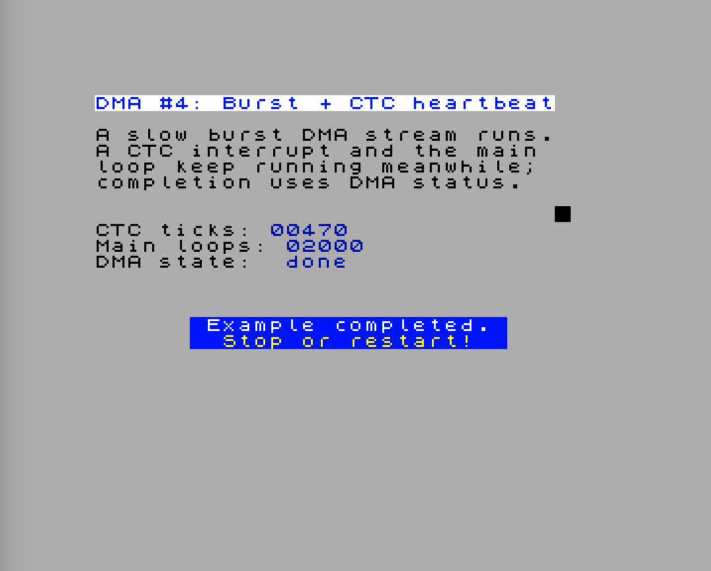
Demo: Keeping the CPU Alive During Burst DMA
The previous demo lets an existing interrupt source break into a continuous DMA transfer. This next one uses the other side of the same idea: the DMA transfer itself is paced as a burst transfer, so the CPU gets the bus back between bytes. While DMA is still active, the main loop updates an attribute cell and a CTC interrupt keeps incrementing a heartbeat counter.
The ZX Spectrum Next FPGA does not expose a zxnDMA “finished” interrupt to normal Z80 code. So this demo deliberately separates the two ideas: CTC proves that interrupts can still run while DMA is active, and the DMA status byte is used to detect completion.
; Extra constants used by the heartbeat demo.
NR_INT_EN_1     .equ $c5
NR_INT_STATUS_1 .equ $c9

CTC_CH0         .equ $183b
CTC_CH1         .equ $193b
CTC_CH2         .equ $1a3b

CTC2_PRIORITY   .equ 5
CTC2_VECTOR     .equ VECTOR_TOP_BITS | (CTC2_PRIORITY << 1)
HEARTBEAT_DMA_DEST .equ $57ff    ; Safe single-byte screen target
HEARTBEAT_DMA_SIZE .equ $8000    ; Long enough to watch the animation
BURST_PRESCALER .equ 255         ; Slowest paced burst transfer
ATTR_ROW7       .equ $5800 + 7 * 32

;==========================================================
; Burst DMA with CTC heartbeat demo
;==========================================================
DmaWithCtcHeartbeat
    Display.PrintTitle(@Title_Heartbeat)
    Display.PrintText(@Instr_Heartbeat)

    di

    ; Keep unrelated interrupt sources quiet for this demo.
    nextreg NR_INT_EN_0,0
    nextreg NR_INT_EN_1,0
    nextreg NR_INT_STATUS_0,$ff
    nextreg NR_INT_STATUS_1,$ff
    nextreg NR_DMA_INT_EN_0,0

    call @ResetCtcChannels

    xor a
    ld (@HeartbeatTicks),a
    ld (@HeartbeatTicks+1),a
    ld (@MainLoops),a
    ld (@MainLoops+1),a
    ld (@AttrCol2),a
    ld (@DmaDoneFlag),a

    ; --- Set up hardware IM2 for CTC channel 2.
    ld a,high(@VectorTable2)
    ld i,a
    im 2
    nextreg NR_INT_CONTROL,VECTOR_TOP_BITS | $01

    ; Enable CTC channel 2 in the Next interrupt controller.
    nextreg NR_INT_EN_1,%00000100
    nextreg NR_INT_STATUS_1,%00000100

    ; CTC cascade for a visible heartbeat:
    ; Ch0: 28 MHz / 16 / 250 = 7000 Hz
    ; Ch1: 7000 Hz / 28      = 250 Hz
    ; Ch2: 250 Hz / 5        = 50 Hz -> 20 ms
    ld bc,CTC_CH2
    ld a,%11000101          ; Interrupt on, counter mode, TC follows
    out (c),a
    ld a,5
    out (c),a

    ld bc,CTC_CH1
    ld a,%01000101          ; Counter mode, TC follows
    out (c),a
    ld a,28
    out (c),a

    ld bc,CTC_CH0
    ld a,%00000101          ; Timer mode, prescaler /16, TC follows
    out (c),a
    ld a,250
    out (c),a

    ; Upload and start a long paced burst DMA stream.
    ld hl,@BurstDmaProgram
    ld b,@BurstDmaProgramEnd - @BurstDmaProgram
    ld c,DMA_PORT
    otir

    ld bc,DMA_PORT
    ld a,$87                ; WR6: Enable DMA
    out (c),a

    ei

`mainLoop
    call @AnimateHeartbeat
    call @ShowHeartbeatCounters

    ld bc,DMA_PORT
    ld a,$bf                ; WR6: Read Status Byte
    out (c),a
    in a,(c)
    bit 5,a                 ; 0 = end of block reached
    jr nz,`mainLoop

    di
    ld a,1
    ld (@DmaDoneFlag),a
    call @ShowHeartbeatCounters

    ; --- Restore the normal interrupt setup.
    nextreg NR_INT_EN_1,0
    nextreg NR_INT_STATUS_1,%00000100
    call @ResetCtcChannels

    ld bc,DMA_PORT
    ld a,$83                ; WR6: Disable DMA
    out (c),a

    nextreg NR_INT_EN_0,1
    nextreg NR_INT_CONTROL,0
    im 1
    ei
    ret

;----------------------------------------------------------
; CTC Channel 2 ISR: heartbeat while burst DMA is active
;----------------------------------------------------------
@Ctc2Isr
    push af
    push hl

    ld hl,(@HeartbeatTicks)
    inc hl
    ld (@HeartbeatTicks),hl

    nextreg NR_INT_STATUS_1,%00000100

    pop hl
    pop af
    ei
    reti

;----------------------------------------------------------
; Main-loop activity while DMA is active
;----------------------------------------------------------
@AnimateHeartbeat
    ld hl,(@MainLoops)
    inc hl
    ld (@MainLoops),hl

    ld a,l
    and $0f
    ret nz

    ld a,(@AttrCol2)
    ld e,a
    ld d,0
    ld hl,ATTR_ROW7
    add hl,de
    ld (hl),%00111000       ; White paper, black ink

    ld a,(@AttrCol2)
    inc a
    and $1f
    ld (@AttrCol2),a

    ld e,a
    ld d,0
    ld hl,ATTR_ROW7
    add hl,de
    ld (hl),%01000111       ; Bright black paper, white ink
    ret

@ShowHeartbeatCounters
    Display.PrintAt(8,0)
    Display.Ink(Color.Black)
    Display.PrintText(@TextHeartbeat)
    ld hl,(@HeartbeatTicks)
    Display.Ink(Color.Blue)
    Display.PrintHLDecimal()

    Display.PrintAt(9,0)
    Display.Ink(Color.Black)
    Display.PrintText(@TextMainLoops)
    ld hl,(@MainLoops)
    Display.Ink(Color.Blue)
    Display.PrintHLDecimal()

    Display.PrintAt(10,0)
    Display.Ink(Color.Black)
    Display.PrintText(@TextDmaState)
    ld a,(@DmaDoneFlag)
    or a
    jr z,`active
    Display.Ink(Color.Blue)
    Display.PrintText(@TextDone)
    ret
`active
    Display.Ink(Color.Blue)
    Display.PrintText(@TextActive)
    ret

@BurstDmaProgram
    .dma reset
    .dma wr0 a_to_b, transfer, @FillByte2, HEARTBEAT_DMA_SIZE
    .dma wr1 memory, fixed
    .dma wr2 memory, fixed, 3t, BURST_PRESCALER
    .dma wr4 burst, HEARTBEAT_DMA_DEST
    .dma wr5
    .dma load
@BurstDmaProgramEnd

;----------------------------------------------------------
; Put CTC channels 0-2 into a known stopped state.
;----------------------------------------------------------
@ResetCtcChannels
    ld a,%00000011          ; D1=1 soft reset, D0=1 control word

    ld bc,CTC_CH0
    out (c),a
    out (c),a

    ld b,high(CTC_CH1)
    out (c),a
    out (c),a

    ld b,high(CTC_CH2)
    out (c),a
    out (c),a
    ret

@FillByte2
    .db $00

@HeartbeatTicks
    .defw 0

@MainLoops
    .defw 0

@AttrCol2
    .db 0

@DmaDoneFlag
    .db 0

    .align 256
@VectorTable2
    .defs CTC2_VECTOR
    .defw @Ctc2Isr
    .defs $100 - CTC2_VECTOR - 2

@Title_Heartbeat
    .defn "DMA #4: Burst + CTC heartbeat"

@Instr_Heartbeat
    .defm "A slow burst DMA stream runs.\x0d"
    .defm "A CTC interrupt and the main\x0d"
    .defm "loop keep running meanwhile;\x0d"
    .defn "completion uses DMA status.\x0d\x0d"

@TextHeartbeat
    .defn "CTC ticks: "

@TextMainLoops
    .defn "Main loops: "

@TextDmaState
    .defn "DMA state:  "

@TextActive
    .defn "active"

@TextDone
.defn "done "Try the DmaInterruptDemo.DmaWithCtcHeartbeat example.
The .dma wr4 burst mode is the important part. With a non-zero Port B prescaler, the DMA engine transfers a byte, waits for the programmed pace, and gives the CPU opportunities to run between paced bytes. This sample uses the slowest prescaler and a long block length so the effect is visible instead of ending immediately.
Both DMA ports are fixed in this demo. Port A repeatedly reads the same fill byte, and Port B repeatedly writes $57FF, a harmless single byte near the end of the ULA bitmap. That avoids clearing the title or trampling over code while still keeping the DMA engine genuinely active for thousands of paced transfers. That is why the main-loop counter and the moving attribute cell keep changing while DMA is still active.
The CTC cascade is the same pattern used in Chapter 5. Channel 0 produces a 7000 Hz pulse stream, Channel 1 divides that to 250 Hz, and Channel 2 divides by 5 and raises an interrupt every 20 ms. If the CTC counter increases before the DMA state changes to done, the CPU has serviced real interrupts during the DMA transfer.
Completion still uses polling:
ld a,$bf                ; WR6: Read Status Byte
out (c),a
in a,(c)
bit 5,a                 ; 0 = end of block reached
That polling is not a weakness of the example; it matches the hardware interface. Use DMA interrupt break-in when another interrupt source must stay responsive during a long transfer, and use status polling when your code needs to know that the DMA block has actually finished.
Practical DMA Patterns and Reference
The demos above show the moving parts in isolation: copying, measuring, interrupt break-in, and paced burst transfers. The rest of the chapter collects the reusable habits you will reach for when building real code: small DMA tables, fixed-source fills, runtime patch points, timing expectations, and a few common traps.
Memory Fill
Filling a block of memory with a constant value is a classic DMA trick. The technique uses Port A in fixed address mode, pointing at a single byte containing the fill value:
; Fill 6144 bytes at 0x4000 with the value stored at FillByte
FillByte:
    .db $00                                 ; fill value — modify before calling DmaFill

dmaFillProgram:
    .dma reset
    .dma wr0 a_to_b, transfer, FillByte, 6144   ; Port A = FillByte label, length = 6144
    .dma wr1 memory, fixed                  ; Port A fixed — reads the same byte every time
    .dma wr2 memory, increment              ; Port B increments through destination
    .dma wr4 continuous, $4000              ; continuous mode, Port B = start of ULA pixels
    .dma wr5
    .dma load
    .dma enable
dmaFillProgram_end:

DmaFill:
    ld hl,dmaFillProgram
    ld b,dmaFillProgram_end - dmaFillProgram
    ld c,$6B
    otir
    ret
The key insight is wr1 memory, fixed: Port A holds the address of FillByte and never advances — the same byte is read 6,144 times while Port B increments through the destination. To change the fill value, write to FillByte before calling DmaFill. The result: the entire screen pixel area is cleared in one DMA operation.
Loading Sprites via DMA
Sprite pattern data needs to get from main memory into the Next’s sprite pattern RAM. The sprite hardware is accessed through I/O ports — you select a pattern slot via port 0x303B, then write pixel data to port 0x5B. Each sprite pattern is 256 bytes (16×16 pixels, 8 bits per pixel). The full sprite memory model and pattern-slot workflow are covered in the Sprites chapter.
; DMA program table — source address and length patched per call
spriteDMAProgram:
    .dma reset
    .dma wr0 a_to_b, transfer           ; base byte only: all follow-bits set
spriteDMASrc:
    .dw 0                               ; Port A address — patched to sprite sheet source
spriteDMALength:
    .dw 0                               ; Block length   — patched to byte count
    .dma wr1 memory, increment
    .dma wr2 io, fixed                  ; Port B = I/O port, fixed address
    .dma wr4 continuous                 ; base byte only: Port B address follows
    .dw $005B                           ; Port B = sprite pattern data port
    .dma wr5
    .dma load
    .dma enable
spriteDMAProgram_end:

; Load sprites: HL = source address, BC = byte count
; Precondition: select the target pattern slot via port 0x303B before calling
LoadSprites:
    ld bc,$303B
    ld a,0                             ; Start at pattern slot 0
    out (c),a

    ld (spriteDMASrc),hl               ; patch source address
    ld (spriteDMALength),bc            ; patch byte count
    ld hl,spriteDMAProgram
    ld b,spriteDMAProgram_end - spriteDMAProgram
    ld c,$6B
    otir
    ret
.dma wr0 a_to_b, transfer without address/length arguments emits only the WR0 base byte with all follow-byte indicator bits set; the two .dw 0 patch labels that follow serve as those follow bytes. Similarly, .dma wr4 continuous without an address argument emits only the WR4 base byte with address follow-bits set; the .dw $005B provides the constant port address.
The sprite hardware auto-increments its internal write pointer each time you write to port 0x5B, so the DMA streams bytes to the same fixed port address while the sprite RAM pointer advances internally.
Audio Transfers
Audio is one of the most important uses for burst DMA, but the full discussion belongs with DAC setup, sample formats, routing, and buffer management. This chapter gives you the DMA building blocks; the DAC and Sample Playback chapter applies them to real sample playback.
For orientation, the two audio-shaped DMA choices are:
| Use case | DMA pacing |
|---|---|
| Simple sample playback | Burst mode with WR2 prescaler |
| Accurate sample clock shared with other timing logic | Burst mode triggered by CTC via NR $CD |
Building a Reusable DMA Helper
The upload sequence — patch any runtime fields, then run OTIR to stream the program table to the DMA port — is short, but wrapping it as a subroutine keeps call sites clean:
; Upload a DMA program table to the zxnDMA port
; HL = pointer to table, B = length in bytes
ExecuteDma:
    ld c,$6B               ; zxnDMA port
.loop:
    ld a,(hl)
    out (c),a
    inc hl
    djnz .loop
    ret
With .dma pragmas, each program table is self-documenting:
; 256-byte memory copy from 0x8000 to 0xC000 — all values static
DmaCopyParams:
    .dma reset
    .dma wr0 a_to_b, transfer, $8000, 256
    .dma wr1 memory, increment
    .dma wr2 memory, increment
    .dma wr4 continuous, $C000
    .dma wr5
    .dma load
    .dma enable
DmaCopyParamsLen = $ - DmaCopyParams
Call it with:
    ld hl,DmaCopyParams
    ld b,DmaCopyParamsLen
    call ExecuteDma
For tables with runtime-patchable fields, label the .dw 0 patch points and write the runtime values before calling:
DmaDynParams:
    .dma reset
    .dma wr0 a_to_b, transfer           ; base byte only — address and length follow
DmaDynSrc:  .dw 0                       ; patched at runtime
DmaDynLen:  .dw 0                       ; patched at runtime
    .dma wr1 memory, increment
    .dma wr2 memory, increment
    .dma wr4 continuous                 ; base byte only — Port B address follows
DmaDynDst:  .dw 0                       ; patched at runtime
    .dma wr5
    .dma load
    .dma enable
DmaDynParamsLen = $ - DmaDynParams
Call with:
    ; HL = source, DE = destination, BC = byte count
    ld (DmaDynSrc),hl
    ld (DmaDynDst),de
    ld (DmaDynLen),bc
    ld hl,DmaDynParams
    ld b,DmaDynParamsLen
    call ExecuteDma
You can define as many program tables as you need and dispatch them all through the same five-instruction ExecuteDma routine.
Timing and Performance Notes
T-State Costs
Each byte transfer costs a read cycle plus a write cycle. The exact timing depends on the source and destination types and the CPU speed:
| Operation | Speed | T-States |
|---|---|---|
| Memory read | 3.5–14 MHz | 3 |
| Memory read | 28 MHz (non-Bank 7) | 4 (wait state) |
| Memory read | 28 MHz (Bank 7) | 3 (no wait state) |
| Memory write | All speeds | 3 |
| I/O port read/write | All speeds | 4 |
SPI port (0xEB) | All speeds | 4 + 16 (SPI wait) |
A typical memory-to-memory byte costs 6 T-states (3 read + 3 write). Memory-to-I/O costs 7 (3 + 4). The SPI port is slow because the FPGA needs time to shift data through the serial interface.
DMA vs LDIR
| Transfer | LDIR | DMA (Continuous) | Speedup |
|---|---|---|---|
| 256 bytes, mem→mem | 5,376 T | ~1,536 T | 3.5× |
| 6,144 bytes (ULA screen) | 129,024 T | ~36,864 T | 3.5× |
| 16,384 bytes (memory bank) | 344,064 T | ~98,304 T | 3.5× |
The DMA’s advantage is consistent: roughly 3.5× faster for memory-to-memory copies. But the real win is for I/O transfers — loading sprite data through a port, streaming audio to a DAC — where LDIR is the wrong tool altogether.
CPU Interaction
During a continuous transfer, the CPU is completely halted. It doesn’t execute instructions and it cannot respond to maskable interrupts while the DMA owns the bus. For very long transfers at the default 3.5 MHz speed, this is rarely a problem — but at 28 MHz with a large block, be aware that the DMA could hold the bus for a noticeable fraction of a frame.
Burst mode solves this by releasing the bus periodically. The CPU gets small windows of execution time between DMA bytes, which is enough to service interrupts and keep background tasks alive.
Common Mistakes and Debugging Tips
Forgetting the Load command. The most common DMA bug. If your transfer goes to the wrong place, or nothing happens at all, check that you issued 0xCF after configuring registers and before enabling.
Wrong port for byte transfer direction. If Port B is configured as I/O with a fixed address, make sure you’re actually using WR2 (base byte ending in 000) and not WR1 (100). The two registers have identical structures but control different ports.
Block length of zero. In zxnDMA mode, a block length of 0 is treated as a zero-byte transfer — nothing happens. In legacy mode (0x0B), a block length of 0 transfers 1 byte. If your code calculates block lengths dynamically, guard against the zero case.
Not resetting before reconfiguration. While you can update individual registers between transfers, starting from a Reset eliminates surprises from leftover state. Unless performance demands it, always Reset first.
Reading status without the Read Status command. The DMA port read returns whatever register is currently in the read sequence. If you haven’t set up the read sequence (with 0xBF or 0xBB + 0xA7), the read may return garbage. Always issue a read command before reading.
Continuous mode during audio. Using continuous mode for audio streaming freezes the CPU for the entire playback. Use burst mode with a prescaler instead — the CPU gets breathing room between samples.
Quick Reference: Common DMA Sequences
Reset and Disable
    ld bc,$6B
    ld a,$C3           ; Reset
    out (c),a
    ld a,$83           ; Disable DMA
    out (c),a
Minimal Memory Copy (A to B, Continuous)
; HL = source address, DE = destination address, BC = byte count
MemCopyDMA:
    ld (memCopySrc),hl
    ld (memCopyDst),de
    ld (memCopyLen),bc
    ld hl,memCopyProgram
    ld b,memCopyProgram_end - memCopyProgram
    ld c,$6B
    otir
    ret

memCopyProgram:
    .dma reset
    .dma wr0 a_to_b, transfer
memCopySrc: .dw 0
memCopyLen: .dw 0
    .dma wr1 memory, increment
    .dma wr2 memory, increment
    .dma wr4 continuous
memCopyDst: .dw 0
    .dma wr5
    .dma load
    .dma enable
memCopyProgram_end:
Memory to I/O Port (A to B, Continuous)
; HL = source address, BC = byte count, DE = 16-bit I/O port address
MemToIODMA:
    ld (ioSrc),hl
    ld (ioLen),bc
    ld (ioDst),de
    ld hl,ioProgram
    ld b,ioProgram_end - ioProgram
    ld c,$6B
    otir
    ret

ioProgram:
    .dma reset
    .dma wr0 a_to_b, transfer
ioSrc:  .dw 0
ioLen:  .dw 0
    .dma wr1 memory, increment
    .dma wr2 io, fixed
    .dma wr4 continuous
ioDst:  .dw 0
    .dma wr5
    .dma load
    .dma enable
ioProgram_end:
The zxnDMA may look intimidating at first — seven register groups, follow bytes, direction bits, operating modes. But once you’ve built a couple of transfers, the pattern becomes automatic: build a .dma program table, patch any runtime fields, and stream it with OTIR. The CPU steps aside, the data flows, and everyone’s happy.
Where Next
- The CTC: Counter/Timer Circuit gives you the timing side of CTC-triggered DMA, including the counter modes used for precise pacing.
- Sprites, Layer 2, and DAC Audio are natural places to use DMA once the byte-shuffling machinery feels familiar.
- I/O Ports and NextRegs and Appendix C: I/O Ports Reference are the maps to keep open when a transfer targets hardware ports instead of memory.