Memory Architecture: ROM, RAM, Banks, and the MMU
The Z80 has sixteen address lines and can see exactly 64 KB at a time. The ZX Spectrum Next has 2 MB of RAM. Bridging that 32× gap is the job of the MMU — the Memory Management Unit baked into the FPGA — and getting comfortable with it is the foundation for nearly every later chapter. Layer 2 bitmaps, sprite patterns, AY tracker data, sample buffers for the DACs, even the dot-command loader from the storage world: all of them live in pages that you have to consciously map in.
The good news: the Next’s memory model is regular, and once you internalise four small words — region, bank, page, slot — the rest is bookkeeping. The bad news: those four words are used interchangeably (and incorrectly) in a lot of online material. We’ll fix that here, and stick to one definition for each throughout the rest of the book.
The Address-Space Problem
The Z80 puts a 16-bit address on the bus. The Next stores 21 bits’ worth of memory. Something has to translate one to the other every single time the CPU reads or writes — and that “something” is the MMU.
Concretely: when the CPU executes ld a,(hl) with HL = $5000, the Z80 places $5000 on the address bus. The MMU sees that address, looks up “what page is currently mapped at $4000–$5FFF?”, and replaces the top three bits of the address with the page number. The result is a 21-bit physical address into the 2 MB pool, and that’s the address that actually goes to RAM.
That’s the whole story. Everything else in this chapter is detail.
RAM All the Way Down
Here’s something that might surprise you: the Next has no ROM chips. None. The FPGA uses SRAM — regular read/write memory — for everything, including the area you access when slots 0 and 1 hold $FF.
What we call “ROM” is SRAM that the FPGA pre-loads at power-on from data baked into its configuration bitstream. Once loaded, those addresses behave like ROM only because the FPGA’s access logic refuses write operations to that region — not because the memory itself is physically read-only. The “ROM lock” is a rule enforced in FPGA fabric, not a hardware property of the chip.
Why does this matter?
- The alt-ROM mechanism makes immediate sense: swapping in an alt-ROM is just telling the FPGA to use a different SRAM region when slot 0/1 is accessed. Same chip, same bus, different address range.
- The divMMC trick works the same way: when a trap address is hit, divMMC re-routes slots 0/1 to yet another SRAM region — the divMMC firmware area — without touching a single MMU register.
- Everything shares one bus. The Z80, the ULA, the DMA engine, and the Copper all read and write the same physical SRAM. There is no separate ROM bus, no FLASH chip. Understanding the FPGA physical address layout explains how all subsystems co-exist on the same machine.
The System Region: The First 256 KB
The FPGA’s physical address space runs from $00'0000 to $1F'FFFF — 21 address bits, 2 MB total. The first 256 KB ($00'0000–$03'FFFF) is reserved for ROMs and system firmware. No MMU page number ever maps here; page 0 starts at $04'0000.
Physical address      Size    Contents
──────────────────    ──────  ──────────────────────────────────────
$00'0000–$00'3FFF     16 KB   ROM 0  (128K editor / NextBASIC)
$00'4000–$00'7FFF     16 KB   ROM 1  (128K BASIC)
$00'8000–$00'BFFF     16 KB   ROM 2  (+3 DOS)
$00'C000–$00'FFFF     16 KB   ROM 3  (48K BASIC)
$01'0000–$01'1FFF      8 KB   divMMC ROM
$01'2000–$01'3FFF      8 KB   Reserved
$01'4000–$01'7FFF     16 KB   Multiface ROM/RAM
$01'8000–$01'BFFF     16 KB   Alt ROM 0  (128K-style, used by NextZXOS)
$01'C000–$01'FFFF     16 KB   Alt ROM 1  (48K-style, used by NextZXOS)
$02'0000–$03'FFFF    128 KB   divMMC RAM  (SD card firmware workspace)
──────────────────    ──────  ──────────────────────────────────────
Total system region  256 KB
The four “standard” ROM images in the first 64 KB are the ones you’re probably familiar with. ROM 0 is the 128K editor (also used by NextBASIC); ROM 1 is 128K BASIC; ROM 2 is the +3 DOS; ROM 3 is the original 48K BASIC. The two-bit selector formed by bit 4 of $7FFD and bit 2 of $1FFD decides which one the Z80 sees through slots 0/1.
The alt-ROMs just below that are where NextZXOS lives. At boot, before any user code runs, the FPGA loads NextZXOS into alt-ROM 0 (128K-style) and alt-ROM 1 (48K-style). When NextZXOS is active, the standard ROM images are still present — they’re just not selected. Swap the selector, and the original 48K ROM re-appears at $0000.
The unexpanded vs. expanded Next. A base Next has 1 MB of total SRAM: 256 KB system region + 768 KB of user RAM = 96 user pages. A fully expanded 2 MB Next adds two more 512 KB IC chips, bringing user RAM to 1792 KB = 224 pages (numbered
$00–$DF). Page numbers$E0–$FEare undefined on any hardware;$FFis the ROM sentinel and not a real page.
Everything from $04'0000 upwards is the user-accessible RAM that the MMU’s page numbers actually refer to.
The Vocabulary: Region, Bank, Page, Slot
These four words come up constantly, often in the same paragraph. Pin them down once and you can read any Next reference without confusion.
-
Slot — a chunk of the Z80 address space the MMU treats as a unit. The Next divides the 64 KB Z80 view into eight 8 KB slots, numbered 0–7. Slot 0 is
$0000–$1FFF, slot 1 is$2000–$3FFF, and so on up to slot 7 at$E000–$FFFF. Each slot is mapped independently. -
Page — a chunk of the physical RAM. A page is also 8 KB, and the Next has up to 256 of them on a 2 MB machine. Page numbers fit in a single byte (
$00–$FF). The MMU’s job, ultimately, is to decide which page sits in which slot. -
Bank — a 16 KB chunk of physical memory, named for historical reasons. The 128K Spectrum had eight banks (Bank 0 through Bank 7); the Next has more, but the word “bank” still refers to a 16 KB chunk. A bank is two consecutive pages. Bank
Nlives in pages2Nand2N+1. So Bank 5 is pages 10 and 11, Bank 2 is pages 4 and 5, Bank 7 is pages 14 and 15. You’ll see “bank” used most often when an old port (like$7FFD) is involved, because those legacy ports think in 16 KB chunks. -
Region — a 64 KB chunk of physical memory, selected by the top bits of the 21-bit physical address. There are 32 regions in 2 MB. You’ll meet them once when we look at the address translation formula, and then almost never again — the MMU presents the page-number abstraction so you don’t have to think in regions.
The cheat sheet. Slots are in Z80 space. Pages, banks, and regions are in physical space. A slot holds one page. A bank is two pages. A region is eight pages.
The Physical Map
The system region takes care of itself. Here’s the user-accessible RAM — the memory the MMU’s page numbers actually point to — on a fully expanded 2 MB Next:
Page    Bank    Address (physical)   Contents
─────   ────    ──────────────────   ────────────────────────────────
0–1     Bank 0  $04'0000 – $04'3FFF  RAM (was Bank 0 on 128K)
2–3     Bank 1  $04'4000 – $04'7FFF  RAM (was Bank 1 on 128K)
4–5     Bank 2  $04'8000 – $04'BFFF  RAM (was Bank 2 on 128K)
6–7     Bank 3  $04'C000 – $04'FFFF  RAM (was Bank 3 on 128K)
8–9     Bank 4  $05'0000 – $05'3FFF  RAM (was Bank 4 on 128K)
10–11   Bank 5  $05'4000 – $05'7FFF  ULA screen 0 (Bank 5)
12–13   Bank 6  $05'8000 – $05'BFFF  RAM
14–15   Bank 7  $05'C000 – $05'FFFF  ULA shadow screen (Bank 7)
16–223  Bank 8+ $06'0000 – $1B'FFFF  RAM (Next-only banks)
─────────────────────────────────────────────────────────────────────
                                     (page numbers $E0–$FF reserved)
The two pages worth memorising are 10 and 11 (Bank 5) — that’s where the classic ULA bitmap and attributes live, and you’ll see those page numbers turn up as if they were folklore. Pages 14 and 15 (Bank 7) are the shadow screen, used for double-buffered ULA rendering.
Banks 5 and 7 are physically special: unlike every other user page, which lives in external SRAM, these two banks are stored in FPGA Block RAM (BRAM) — fast internal memory built into the FPGA chip itself. BRAM is dual-ported: the CPU and the ULA/tilemap renderer each get their own independent port and can access the same memory simultaneously without blocking each other. This is how the ULA reads screen data for every scanline without pausing the CPU at all. One caveat: only 8 KB of Bank 7 is backed by BRAM (page 14, the shadow screen itself); page 15 falls back to external SRAM, which is why the Timex hi-res video modes cannot be located in Bank 7.
The ROMs (the original 48K ROM, the 128K editor and BASIC ROMs, the +3 ROMs, plus the divMMC and alt-ROMs) live separately. They aren’t pages — they’re swapped over the top of slots 0 and 1 by a separate mechanism. We’ll come back to them.
The MMU Registers
The MMU itself is just eight bytes, exposed as NextRegs $50 through $57:
| NextReg | Slot | Z80 address range | What it holds |
|---|---|---|---|
$50 | 0 | $0000–$1FFF | page number for slot 0 |
$51 | 1 | $2000–$3FFF | page number for slot 1 |
$52 | 2 | $4000–$5FFF | page number for slot 2 |
$53 | 3 | $6000–$7FFF | page number for slot 3 |
$54 | 4 | $8000–$9FFF | page number for slot 4 |
$55 | 5 | $A000–$BFFF | page number for slot 5 |
$56 | 6 | $C000–$DFFF | page number for slot 6 |
$57 | 7 | $E000–$FFFF | page number for slot 7 |
Each register holds a single byte: the page number that’s mapped into that slot right now. Writing a new value re-maps the slot instantly — the next memory access from the CPU sees the new page.
The 256 possible values fall into three ranges:
-
$00–$DF(0–223) on a fully expanded 2 MB Next — valid user RAM pages. On a less-than-fully-expanded Next the ceiling is lower: 96 pages ($00–$5F) on a base unexpanded machine, 160 pages ($00–$9F) with one expansion IC fitted. The formula is: available pages = installed user RAM in KB ÷ 8. -
$E0–$FF— out-of-range; all 32 values behave identically. In slots 0–1 the hardware falls back to the currently selected ROM image —$FFis just the conventional spelling of “give me ROM here”. In slots 2–7 no memory is selected; the CPU reads$FFfrom idle bus pull-ups on real hardware, or$7E(aLD A,(HL)opcode) as a diagnostic marker in Klive. The default at boot is$50 = $FF,$51 = $FF, giving the ROM view across$0000–$3FFFthat 48K software expects.
NextReg or
nextreg? You can poke$50–$57either through ports$243B/$253B(the universal NextReg path covered in I/O Ports and NextRegs) or with the Z80Nnextreginstruction. The Z80N form is shorter and faster —nextreg $52,ais two bytes and a handful of T-states — so it’s what you’ll see in most Next code.
Address Translation by Example
Here’s how the MMU turns a Z80 address into a physical one. Say slot 2 ($52) contains $0A, meaning page 10, and the CPU reads from $5234:
- Slot selection. Z80 address bits [15:13] =
010= 2 → look up MMU register 2 ($52). - Page base.
$52=$0A= page 10 → FPGA physical base =$04'0000+ 10 ×$2000=$05'4000. - Offset. Z80 address bits [12:0] =
$1234(the position within the 8 KB page). - Result.
$05'4000+$1234=$05'5234.
Page 10 is the first half of Bank 5, so the CPU just read from the byte at offset $1234 of the ULA screen bitmap. (The pixel byte for column 8 of row 18, if you want to be exact.)
The formal version, for completeness:
slot      = (Z80_addr >> 13) & 0x07
offset    = Z80_addr & 0x1FFF
page      = MMU[slot]                 ; one of NextRegs $50–$57
physical  = 0x040000 + (page << 13) + offset   ; FPGA physical address
That’s the entire MMU. Eight registers, four lines of pseudocode.
Memory Decoding Priority
The MMU is not the only mechanism that can intercept a Z80 memory access. Layer 2 mapping, divMMC trapping, the Multiface, and the boot ROM can all claim an address before the MMU gets a say. When more than one is active simultaneously, a fixed priority chain decides the winner.
The Next divides the Z80 address space into three zones with different priority rules:
Slots 0–1 ($0000–$3FFF) — the busiest zone
This is where the most overriding happens. From highest priority to lowest:
- Boot ROM. At cold power-on the FPGA maps its own initialisation code here. It disappears before any user code runs.
- Multiface. The Multiface peripheral (snapshot/trainer device) overrides these slots when activated.
- divMMC. When the CPU fetches an instruction from a trap address —
$0000,$0008,$0038,$0066,$04C6,$0562, and a handful of others — divMMC can hijack slots 0/1. It stays mapped until the firmware explicitly leaves automap, usually throughRETNor the$1FF8–$1FFFexit window. - Layer 2 mapping. Since core 3.0, Layer 2’s read and/or write mapping can be enabled for the
$0000–$BFFFregion, redirecting accesses to the Layer 2 bank in SRAM. Read and write are controlled independently. - MMU (NextRegs
$50/$51). The page numbers you put here, unless any of the above fired first. - Config mode / ROMCS. Expansion bus signals that external peripherals can assert (uncommon in practice).
- ROM (when MMU =
$FF). The final fallback: if the MMU register holds$FFand nothing higher in the chain fired, the selected ROM image from the system region is returned.
Slots 2–3 ($4000–$7FFF)
Only two mechanisms compete:
- Layer 2 mapping — read and/or write can be redirected to the Layer 2 SRAM bank.
- MMU (NextRegs
$52/$53).
Layer 2 write mapping to this region is the key technique for building the Layer 2 framebuffer: you enable it, write pixels directly at $4000–$7FFF, the FPGA silently redirects every write to the Layer 2 bank, and the MMU page in those slots is left untouched. Full details are in Layer 2.
Slots 4–7 ($8000–$FFFF)
The MMU is the only authority. Whatever page number you put in NextRegs $54–$57 is what the CPU sees — no Layer 2 mapping, no divMMC, no Multiface. This is why slots 4/5 are the safe scratch window for user code: you get the whole 16 KB to yourself with no surprises.
What this means in practice. You rarely have to think about this priority chain. The two cases that bite programmers are: (a) don’t rely on the contents of slots 0/1 while divMMC might be active — an unexpected trap will briefly re-map them; and (b) if Layer 2 write mapping is enabled, writes to slots 0–3 hit the Layer 2 buffer rather than whatever RAM page the MMU says is there. Useful when intentional, mysterious when not.
Mapping a Page Yourself
Reading and writing the MMU is identical to reading and writing any other NextReg. The simplest case — map
page $0A (Bank 5, low half) into slot 6 — is one Z80N instruction:
nextreg $56,$0A ; slot 6 ($C000-$DFFF) now sees page 10After that, writing to $C000 with slot 6 mapped to page $0A hits the same physical address as writing to $4000 with the default mapping — both end up at physical $05'4000.
Why does the demo use slot 6? All chapter examples run as NEX files, which place unbanked code into Bank 2 starting at $8000. Slots 4 and 5 hold this Bank 2 code (entry point, helpers, examples, and stack), so they’re off-limits. This is what the remaining slots look like when the demo runs:
- Slots 0/1 (MMU0/1,
$0000–$3FFF) hold the ROM. Every helper usesRST $10for character output; paging out either slot kills screen I/O. - Slot 2 (MMU2,
$4000–$5FFF) maps page 10 — the ULA pixel and attribute data. Replacing it disconnects writes from the visible screen. - Slot 3 (MMU3,
$6000–$7FFF) maps page 11. The ROM treats pages 10 and 11 as a contiguous bank; swapping either half can confuse routines that work across both. - Slots 6/7 (MMU6/7,
$C000–$FFFF) map Bank 0, used by the ROM for BASIC workspace, channel descriptors, and system stack. Replacing either while a ROM call is in progress corrupts those structures.
Slot 6 is the safest choice: it’s less likely to interfere with the ROM or running code. You can map any page into any slot, but picking one in active use risks crashes or unexpected behavior.
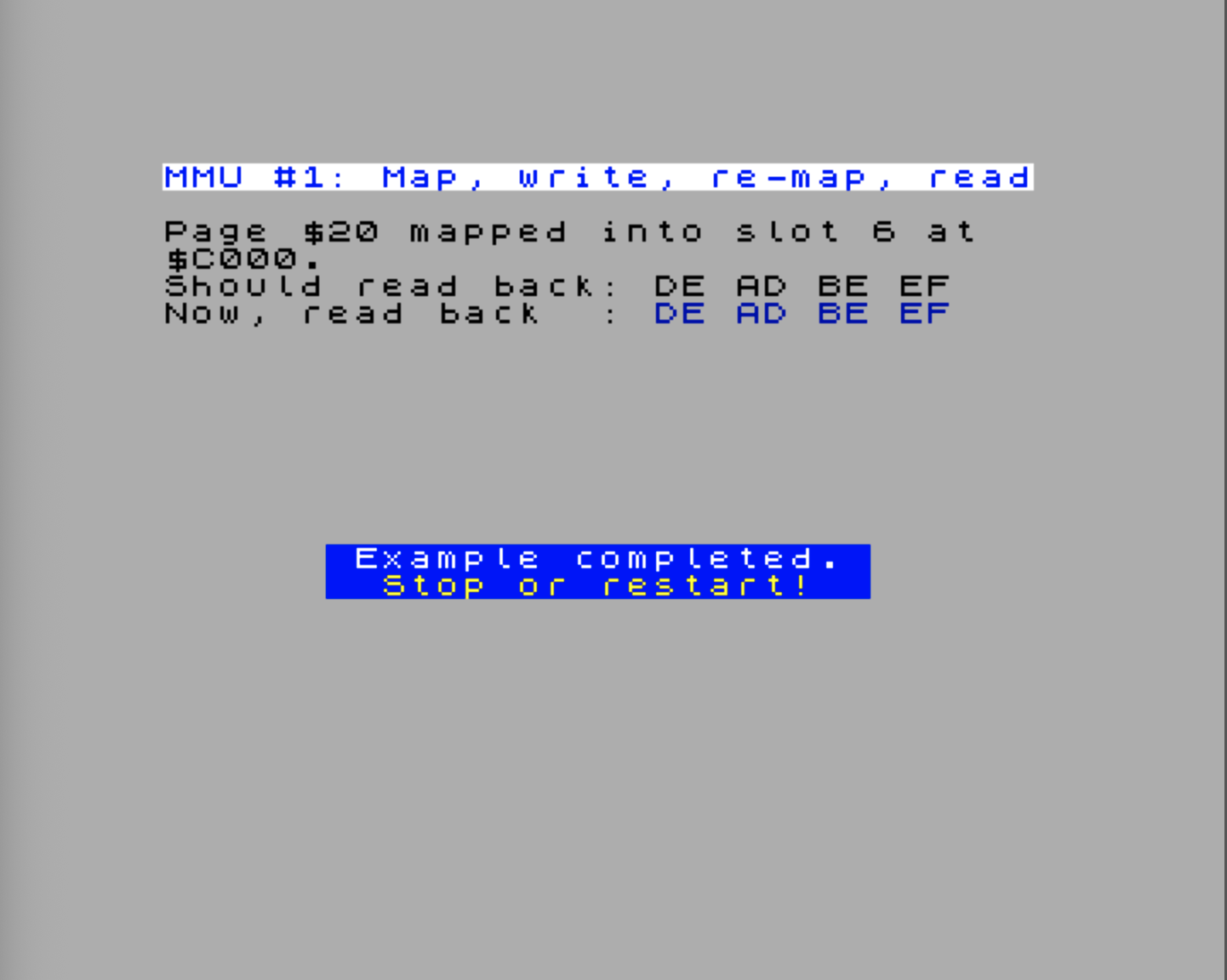
Here’s a small Klive demo that does the round trip: it picks an arbitrary page, maps it into slot 6, writes a marker, then maps it back out and confirms the marker is still there when we map it back in.
MMU6_REG    .equ $56
SLOT6_START .equ $c000

;==========================================================
; Use the MMU
;==========================================================
MmuRoundTrip
    Display.PrintTitle(@Title_MmuRoundTrip)
    Display.PrintText(@Instr_MmuRoundTrip)
    Display.PrintText(@Result_MmuRoundTrip)
    Display.Ink(Color.Blue)

    ; --- Save current MMU6 so we can restore it
    ld a,MMU6_reg
    GetNextReg(MMU6_REG)      ; A := current value of MMU6
    ld (@SavedMmu6),a

    ; --- Map page $20 into slot 6 ($C000-$DFFF)
    nextreg MMU6_REG,$20

    ; --- Write a marker pattern at the start of the page
    ld hl,SLOT6_START
    ld (hl),$DE
    inc hl
    ld (hl),$AD
    inc hl
    ld (hl),$BE
    inc hl
    ld (hl),$EF

    ; --- Map something else there (page 10, Bank 5 low) so we can prove
    ;     the marker isn't just sitting in slot 6 by accident
    nextreg MMU6_REG,$0A

    ; --- Now map page $20 back in...
    nextreg MMU6_REG,$20
    ld hl,SLOT6_START
    call PrintSignature

    ; --- Restore MMU6
    ld a,(@SavedMmu6)
    nextreg MMU6_REG,a                ; select MMU6
    ret

PrintSignature
    call @PrintHLContent
    inc hl
    call @PrintHLContent
    inc hl
    call @PrintHLContent
    inc hl
    jp @PrintHLContent

@PrintHLContent
    push hl
    ld a,(hl)
    Display.PrintAHexadecimal()
    ld a,' '
    rst $10
    pop hl
    ret

@SavedMmu6
    .defb 0

@Title_MmuRoundTrip
    .defn "MMU #1: Map, write, re-map, read"
@Instr_MmuRoundTrip
    .defm "Page $20 mapped into slot 6 at\x0D$C000.\x0D"
    .defn "Should read back: DE AD BE EF\x0D"
@Result_MmuRoundTrip
.defn "Now, read back : "A real program almost always saves and restores the MMU registers it touches. Other code — the ROM, NextZXOS, an interrupt handler — may rely on a particular slot being mapped a specific way. The pattern in the example above (read the current value, do your work, write it back) is the standard idiom.
Try the MmuDemo.MmuRoundTrip example.
Legacy Paging: $7FFD, $1FFD, $DFFD
If the MMU is so clean, why are there also three legacy paging ports?
Compatibility. A 128K Spectrum game that writes to $7FFD to swap a bank into the top 16 KB has to keep working on the Next, even though the Next’s hardware speaks MMU page numbers internally. The Next solves this the only sensible way: it intercepts writes to the legacy paging ports and translates them into MMU updates.
Here’s the cheat sheet for the three legacy ports:
| Port | Origin | What a write does |
|---|---|---|
$7FFD | 128K Spectrum | bits 0–2: bank in slot 6/7; bit 3: shadow screen; bit 4: ROM select; bit 5: lock paging |
$1FFD | +3 / +2A | bit 0: AllRAM mode; bits 1–2: special config and ROM-MSB |
$DFFD | Next | extends the bank selector with bit 3 (and more), giving a 7-bit bank number to slot 6/7 |
The mapping for the most common case — a $7FFD write — is exactly what you’d expect:
OUT ($7FFD),A    with A = ...001 0101  (bank 5, bit 4 = 1, ROM 1 selected)
                                ^^^^^
                                bank LSBs = 5

→ MMU6 := 2 × 5     = 10        ; low half of bank 5  → slot 6
→ MMU7 := 2 × 5 + 1 = 11        ; high half of bank 5 → slot 7
(Plus updates to the ROM selector and the shadow-screen flag — but the MMU effect is just those two slot writes.)
The $DFFD port is the Next’s extension. It carries the upper bits of the bank number, so $7FFD | $DFFD together can address any of the Next’s banks, not just the original eight. Writing both ports gives you a 7-bit (or wider) bank index that the MMU then expands into a pair of page numbers in slots 6 and 7.
Reading Back Legacy Paging State
The legacy paging ports are write-only — there is no way to read them back from I/O space. On original hardware, reading from $7FFD returns whatever was last on the data bus; on the Next it’s similarly meaningless. But if you need to know the current bank and ROM selector, you face a problem: other code (interrupt handlers, a loader) may have changed them, and you need to restore the state later.
On original Spectrum 128/2/3 hardware, the last value written to $7FFD was also stored in the system variable BANKM at address $5B5C, letting code recover the paging state. The NextReg mirrors solve this on the Next, but it’s worth knowing if you’re studying or porting code from classic 128K systems.
The Next solves this with NextReg $8E (Spectrum 128K Memory Mapping), which mirrors the legacy port state. When you write to $7FFD or $1FFD, the FPGA updates this register so the values are queryable:
- bit 7 — reflects port
$DFFDbit 0 - bits 6:4 — reflect port
$7FFDbits 2:0 (bank number) - bit 3 — read-only in the register
- bit 2 — reflects port
$1FFDbit 0 (paging mode) - bit 0 — reflects port
$7FFDbit 4 (ROM selector) or port$1FFDbit 1 (RAM selector) depending on paging mode
Additionally, NextReg $69 bit 6 (Display Control 1) mirrors the shadow screen bit of $7FFD bit 3, giving you another way to read or write the shadow screen state.
You can read these NextRegs at any time to discover the last value written to the legacy ports, even if intervening code has modified them. The pattern is: read the register, save it, do your work, write it back.
The $DFFD bits 1–3 (upper RAM bank extension) are write-only with no NextReg read path. However, you can recover the effective bank by reading MMU slot NextRegs $56 and $57, which always reflect the actual 8 KB pages visible at $C000–$FFFF. The 16 KB bank number is simply MMU6_page >> 1 (pages are paired as 2N / 2N+1 per bank).
Sidebar: don’t mix-and-match. If you’ve taken control of slots 6 and 7 by writing MMU6/MMU7 directly, a stray
$7FFDwrite will clobber your mapping — because the FPGA will faithfully translate the legacy write into MMU writes that overwrite yours. Either commit to MMU-only, or commit to legacy-port-only, in any given chunk of code. (The Next manual calls this “the golden rule of paging”.)
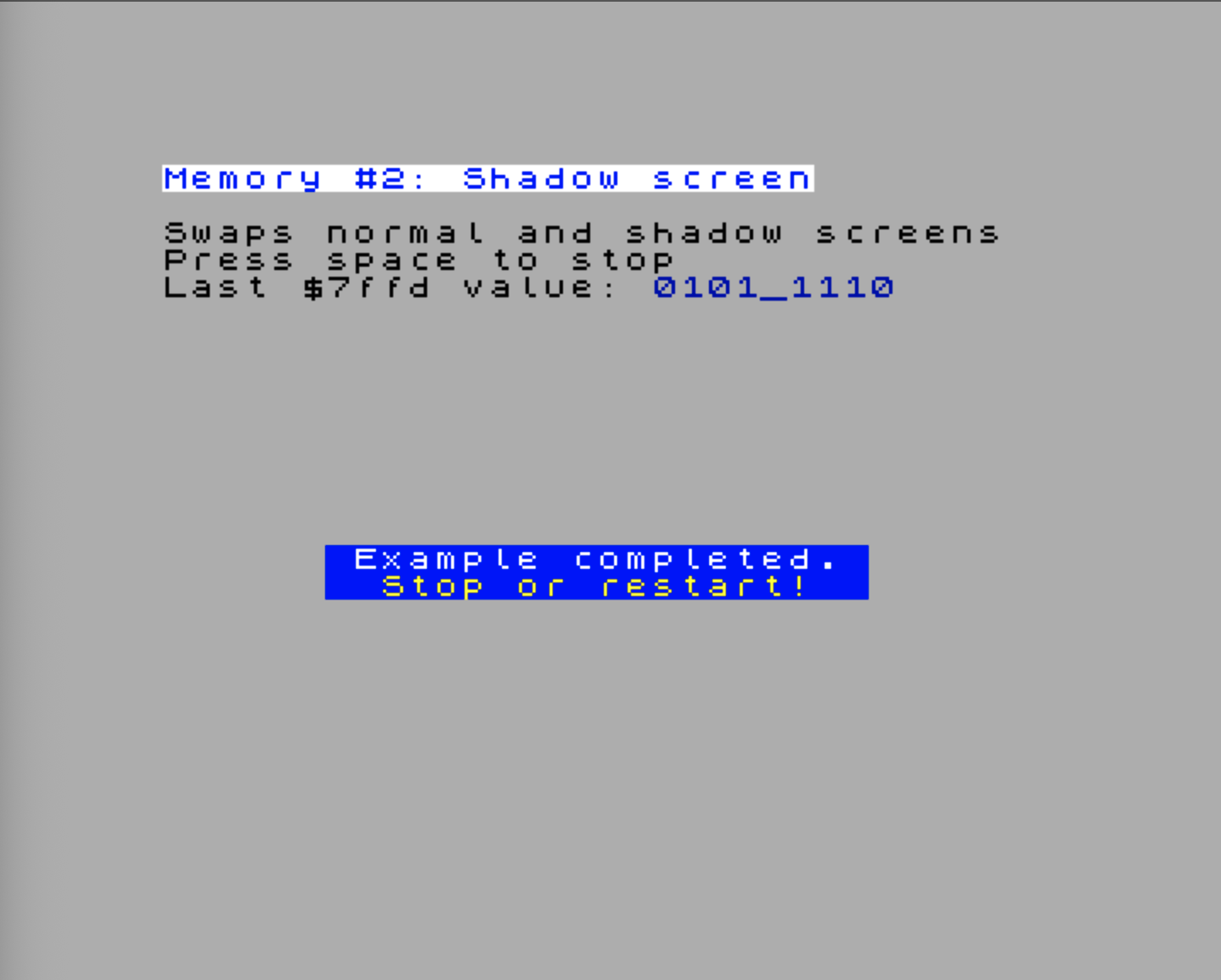
Demo: Toggling the Shadow Screen with $7FFD
This demo illustrates the complete lifecycle of the $7FFD legacy paging port. It copies the current screen to the shadow screen bank, creates a green attribute stripe there, then toggles between normal and shadow screens with $7FFD writes (once per halt), creating a visible flashing stripe. The demo also reads NextReg $8E to discover the current paging state, and saves/restores MMU6 to avoid interfering with other memory mappings.
The key point: the demo never reads from $7FFD itself — it only reads from NextRegs $8E and $69 to discover the current paging state. This demonstrates that the legacy port is write-only and that NextReg mirrors are how you query its state.
MMU6_REG    .equ $56

;==========================================================
; Toggle the shadow screen using $7FFD
;==========================================================
ShadowScreen
    Display.PrintTitle(@Title_ShadowScreen)
    Display.PrintText(@Instr_ShadowScreen)

    Display.Ink(Color.Blue)
    call @Get7ffdStatus         ; Read current $7ffd state via NextRegs
    ld (@Last7ffd),a            ; Save it
    Display.PrintABinary()      ; Display it

    ; --- Save current MMU6 so we can restore it later
    ld a,MMU6_reg
    GetNextReg(MMU6_REG)        ; A := current value of MMU6
    ld (@SavedMmu6),a

    ; --- Copy the current screen to the shadow screen bank
    nextreg MMU6_REG,$0e
    ld hl,$4000                 ; Start of visible screen (bank 5 low)
    ld de,$c000                 ; Shadow screen paged into slot 6
    ld bc,$1b00                 ; Screen size (pixels + attributes)
    ldir

    ; --- Create a green attribute stripe in the shadow screen
    ld hl,$d900
    ld de,$d901
    ld bc,$1f
    ld (hl),attr(Color.Green, Color.Green)
    ldir

    ; --- Restore original MMU6 content
    ld a,(@SavedMmu6)
    nextreg MMU6_REG,a

    ; --- Toggle shadow screen on and off each time we halt
    ld bc,$7ffd
    ei
`swap
    ld a,(@Last7ffd)
    xor $08                     ; Toggle shadow screen bit
    out (c),a
    ld (@Last7ffd),a
    halt                        ; Wait for interrupt
    ld a,$7F                    ; Check Space key
    in a,($FE)
    bit 0,a
    jr nz,`swap

    ; Turn off shadow screen and exit
    ld a,(@Last7ffd)
    res 3,a
    out (c),a
    ret

@Get7ffdStatus
    GetNextReg($8e)             ; Read NextReg $8E (Spectrum 128K Memory Mapping)
    and $75                     ; Mask out irrelevant bits
    ld d,0                      ; Start with bit 4 of $7ffd = 0
    bit 2,a                     ; AllRAM mode active?
    jr nz,`bit4Done             ; If so, bit 4 stays 0
    bit 0,a                     ; ROM selector bit set?
    jr z,`bit4Done              ; If not, bit 4 stays 0
    ld c,$10                    ; Set bit 4 = 1
`bit4Done
    sla a                       ; Shift $8E bits 6:4 → bits 2:0
    sla a
    sla a
    sla a
    or d                        ; Insert bit 4 of $7ffd
    ld d,a                      ; Save reconstructed $7ffd value
    GetNextReg($69)             ; Read NextReg $69 (Display Control 1)
    bit 6,a                     ; Shadow display enabled?
    ld a,d                      ; Restore $7ffd value
    ret z                       ; If shadow off, return
    set 3,a                     ; If shadow on, set bit 3
    ret

@Last7ffd
    .db 0

@SavedMmu6
    .defb 0

@Title_ShadowScreen
    .defn "Memory #2: Shadow screen"
@Instr_ShadowScreen
    .defm "Swaps normal and shadow screens\x0d"
    .defm "Press space to stop\x0d"
.defn "Last $7ffd value: "Try the LegacyMemDemo.ShadowScreen example.
The demo showcases the $7FFD lifecycle:
-
Reading the state.
call @Get7ffdStatusreconstructs the last$7FFDvalue by reading NextRegs$8Eand$69. This proves you can always recover paging state without I/O reads. -
Toggling shadow-screen bit. The core loop reads
last7ffd, XORs with$08to flip bit 3, and writes back to$7FFD. Bit 3 controls whether the shadow screen (banks 14–15) or normal screen (banks 10–11) is visible. Toggling it on eachhaltproduces the flashing stripe. -
Write-only I/O. The code writes to
$7FFDbut never reads from it — you cannot read a legacy paging port. The NextReg mirrors ($8Eand$69) are the only way to query the current state. -
Save-restore pattern. At the end, the code clears bit 3 and writes back to
$7FFD, restoring the normal screen. This is the standard pattern: read, modify, restore — ensuring you don’t clobber state that other code relies on.
In essence, this demo illustrates why NextReg mirrors exist: to bridge the gap between legacy write-only ports and the need to preserve and restore paging state.
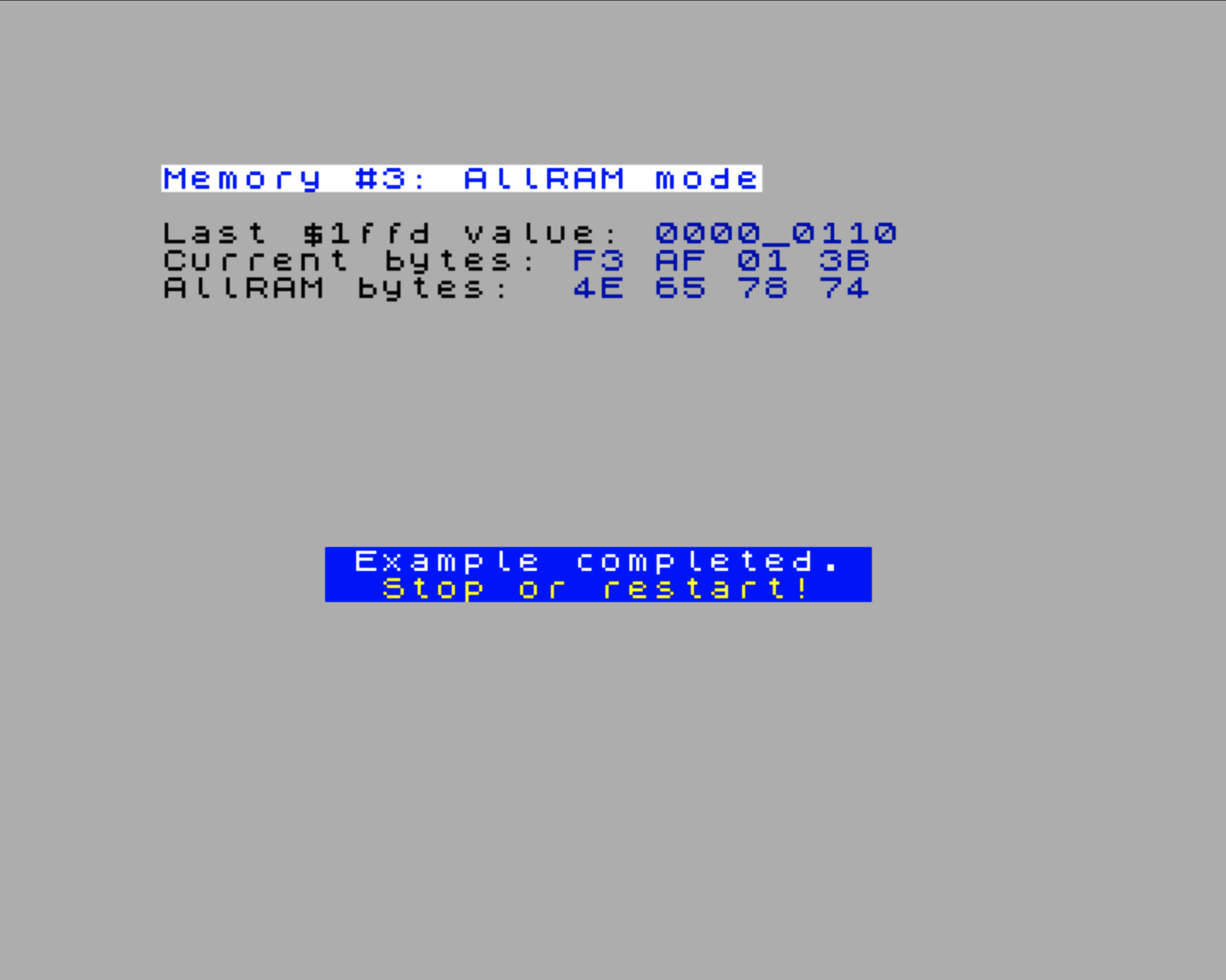
Demo: AllRAM Mode with $1FFD
Setting Bit 0 of $1FFD to 1 puts the Next into “AllRAM mode”, where the ROM is disabled and the entire
$0000–$3FFF range is available for RAM. This is a common mode for loading a custom OS or game engine,
because it gives you the full 64 KB of RAM to work with — but it also means you have to provide your own
reset vector and interrupt handlers, since the ROM is no longer there to catch those.
In AllRAM mode, Bit 1 and Bit 2 of $1FFD determine the configuration of the four 16 KB banks that would
normally be occupied by the ROM. The exact mapping depends on the combination of these bits:
| Bit 2/1 | $0000–$3FFF | $4000–$7FFF | $8000–$BFFF | $C000–$FFFF |
|---|---|---|---|---|
| 00 | Bank 0 | Bank 1 | Bank 2 | Bank 3 |
| 01 | Bank 4 | Bank 5 | Bank 6 | Bank 7 |
| 10 | Bank 4 | Bank 5 | Bank 6 | Bank 3 |
| 11 | Bank 4 | Bank 7 | Bank 6 | Bank 3 |
Our demo examples run as NEX files with code in Bank 2, so the AllRAM configuration that keeps Bank 2 in the upper half of the address space (bits 2/1 = 00) is the one that works with our setup. The other configurations are useful in other contexts but require adjusting where code and data are placed.
This demo makes the effect of AllRAM mode tangible. It reads the first four bytes at $0000–$0003 in normal mode (where the ROM is mapped), then switches to AllRAM mode (Bank 0 mapped at $0000), reads the same four bytes again, and restores the original paging state. The two sets of bytes will differ — proving that a different physical page is now visible at the same address. The @Get1ffdStatus helper reconstructs the current $1FFD state from NextReg $8E, since the port itself is write-only.
;==========================================================
; Demonstrate AllRAM configuration
;==========================================================
AllRam
    Display.PrintTitle(@Title_AllRam)
    Display.PrintText(@Instr_AllRam)

    Display.Ink(Color.Blue)
    call @Get1ffdStatus     ; Get $1ffd status
    ld (@Last1ffd),a        ; Save it
    Display.PrintABinary()  ; Display it
    Display.NewLine()
    Display.Ink(Color.Black)

    ; Display current bytes $0000-0003
    Display.PrintText(@Instr_AllRam2)
    Display.Ink(Color.Blue)
    ld hl,$0000
    call MmuDemo.PrintSignature
    Display.Ink(Color.Black)
    Display.NewLine()

    ; Set AllRAM using Bank 0/1/2/3
    di
    ld a,$01
    ld bc,$1ffd
    out (c),a

    ; Save AllRAM bytes $0000-$0003
    ld hl,$0000
    ld de,@AllRamBytes
    ld bc,4
    ldir

    ; Restore the original configuration
    ld a,(@Last1ffd)
    ld bc,$1ffd
    out (c),a

    ; Display current AllRAM bytes $0000-$0003
    Display.PrintText(@Instr_AllRam3)
    Display.Ink(Color.Blue)
    ld hl,@AllRamBytes
    call MmuDemo.PrintSignature
    ret

@Get1ffdStatus
    GetNextReg($8e)         ; Get $1ffd status
    and $07                 ; Drop non-$1ffd-relate bits
    bit 2,a                 ; Check for AllRAM mode
    jr z,`allRam
    and $01                 ; Keep only Bit 1
    add a,a                 ; Shift bits to left
    ret
`allRam
    scf
    add a,a                 ; Shift bits to left and set bit 0
    ret

@Last1ffd
    .db 0
@AllRamBytes
    .defs 4

@Title_AllRam
    .defn "Memory #3: AllRAM mode"
@Instr_AllRam
    .defn "Last $1ffd value: "
@Instr_AllRam2
    .defn "Current bytes: "
@Instr_AllRam3
.defn "AllRAM bytes: "Try the LegacyMemDemo.AllRam example.
The demo highlights three aspects of AllRAM mode:
-
Reading
$1FFDstate.call @Get1ffdStatusreconstructs the last$1FFDvalue from NextReg$8E, extracting the paging-mode bit and the AllRAM bank-select bits. The port itself is write-only — this is the only way to discover the current state. -
Switching to AllRAM.
OUT ($1FFD), 1sets bit 0, disabling the ROM and mapping banks 0–3 across the full 64 KB. The bytes at$0000–$0003now come from Bank 0, not the ROM image. The two printed sequences will differ, confirming the switch happened. -
Save-restore pattern. The original
$1FFDvalue is saved before the switch and written back immediately after reading the AllRAM bytes. Leaving AllRAM mode active would break everything — there would be no ROM to handleRSTcalls, interrupts, or the return path.
In essence, this demo is a concrete demonstration of why AllRAM mode is powerful and why you must be deliberate about entering and leaving it: from the moment you write bit 0 of $1FFD, the ROM disappears and you are on your own.
Demo: Using $DFFD to Access More Banks
A 128K Spectrum can only address eight 16 KB banks because $7FFD only has three bank bits. The Next is much bigger than that — up to 1.75 MB of user RAM, organised as 112 banks. $DFFD carries the extra four bits that let legacy code reach all of them.
This demo writes a marker into eight Next-only banks ($08–$0F) and reads them back. Each bank is selected by splitting its 7-bit number across the two ports: bits 2:0 go to $7FFD, bits 6:3 go to $DFFD. The pair together selects a single 16 KB bank into slot 6/7 ($C000–$FFFF).
;==========================================================
; Use $DFFD to access RAM banks above bank 7
;==========================================================
DffdBanks
    Display.PrintTitle(@Title_DffdBanks)
    Display.PrintText(@Instr_DffdBanks)

    ; --- Save $7FFD/$DFFD state via NextReg $8E
    GetNextReg($8e)
    ld (@Saved8e),a

    ; --- Save MMU6/MMU7 — legacy port writes will overwrite them
    GetNextReg($56)
    ld (@SavedMmu6),a
    GetNextReg($57)
    ld (@SavedMmu7),a

    ; --- Write a marker into banks 8..15 at offset 0 of slot 6
    ld e,$08
`writeLoop
    ld a,e
    call @SelectBank          ; Map 7-bit bank A via $7FFD + $DFFD
    ld a,e
    ld ($c000),a              ; Marker = bank number
    inc e
    ld a,e
    cp $10
    jr nz,`writeLoop

    ; --- Restore MMU6/7 so the ROM's $C000+ workspace is back
    ld a,(@SavedMmu6)
    nextreg $56,a
    ld a,(@SavedMmu7)
    nextreg $57,a

    ; --- Read each bank's marker, restore Bank 0, then print it
    Display.Ink(Color.Blue)
    ld e,$08
`readLoop
    push de
    ld a,e
    call @SelectBank
    ld a,($c000)              ; A := marker
    ld d,a                    ; Stash before re-mapping
    ld a,(@SavedMmu6)
    nextreg $56,a
    ld a,(@SavedMmu7)
    nextreg $57,a
    ld a,d
    Display.PrintAHexadecimal()
    ld a,' '
    rst $10
    pop de
    inc e
    ld a,e
    cp $10
    jr nz,`readLoop

    ; --- Commit the saved $7FFD/$DFFD state back through $8E.
    ;     bit 3 = 1 tells the FPGA to apply the bank fields.
    ld a,(@Saved8e)
    or $08
    nextreg $8e,a
    ret

;----------------------------------------------------------
; Map 7-bit bank A into slots 6/7 via $7FFD + $DFFD.
;   bits 2:0 of A  → $7FFD  (low bank bits)
;   bits 6:3 of A  → $DFFD  (high bank bits)
;----------------------------------------------------------
@SelectBank
    and $07
    ld h,a
    call @Get7ffdStatus
    and $f8
    or h
    ld bc,$7ffd
    out (c),a
    rrca
    rrca
    rrca
    and $0f
    ld bc,$dffd
    out (c),a
    ret

@Saved8e
    .db 0
@SavedMmu7
    .db 0

@Title_DffdBanks
    .defn "Memory #4: $DFFD bank extension"
@Instr_DffdBanks
    .defm "Markers in banks 8..F\x0d"
.defn "Read back:\x0d"Try the LegacyMemDemo.DffdBanks example.
Four things are worth noticing:
-
Splitting the bank number. The 7-bit bank index is split across two ports because
$DFFDwas bolted on top of$7FFDto extend the original 3-bit bank field rather than replace it. Code that already wrote$7FFDkeeps working unchanged; new code adds a single extraoutto$DFFDto reach the upper banks. -
Preserving the non-bank bits of
$7FFD.$7FFDholds more than the bank number — bits 7:3 carry the ROM selector, the shadow-screen flag, and the paging lock. A naïve implementation that writes only the three bank bits would silently clobber all of them, switching the visible ROM and resetting the shadow-screen state.@SelectBankavoids this by calling@Get7ffdStatusfirst to read the current$7FFDvalue, masking out bits 2:0 (and $f8), then ORing in the new bank bits before writing back. This is the correct, safe pattern whenever you use$7FFDto update just the bank. -
Restoring MMU6/7 before any ROM call. Once we map bank 8+ into slot 6/7, the ROM’s BASIC workspace and channel area at
$C000–$FFFFare gone.RST $10will dereference garbage and crash. The pattern is to read the marker into a register, restore Bank 0 to slots 6/7, then call the print routine. -
Closing through
$8E, not the ports. Bit 3 of$8Esays “apply the bank fields on this write”. Setting it lets us push the saved bank state back in a singlenextreginstruction, restoring$7FFD,$DFFD, MMU6 and MMU7 all at once. This is much tidier than reissuingoutinstructions to both ports.
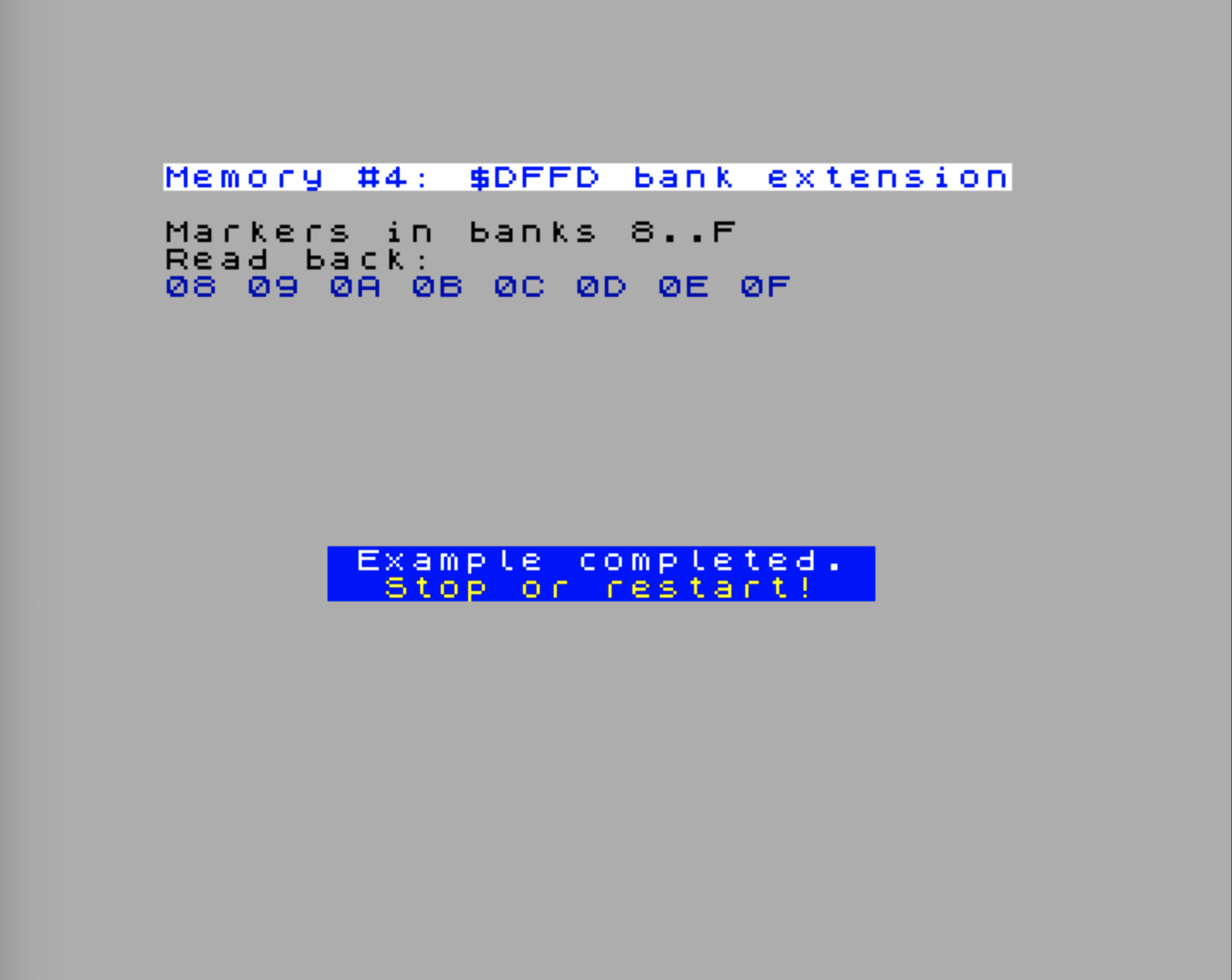
On a base 1 MB Next some of the higher banks ($08–$0F here are still within the safe range) won’t exist. If you walk past the installed RAM ceiling, writes silently disappear and reads return undefined data — exactly the same behaviour as out-of-range MMU page numbers.
ROMs and the Alt-ROM Mechanism
When MMU0 or MMU1 contains $FF, the slot reads from ROM rather than RAM. But which ROM?
The Next ships with the original 16 KB Spectrum 48K ROM, the two 128K ROMs (editor + BASIC), and the two +3 ROMs (DOS + BASIC). One of these is selected at any moment by a combination of:
$7FFDbit 4: low bit of the ROM selector (the 128K original)$1FFDbits 1–2: high bits and special-config (the +3 extension)
In addition, the Next reserves two 16 KB SRAM regions for alt-ROMs — alt-ROM 0 (128K-style, physical $01'8000–$01'BFFF) and alt-ROM 1 (48K-style, physical $01'C000–$01'FFFF). These are regular SRAM, not baked-in firmware: their contents can be written by user code at runtime and then presented to the CPU as if they were ROM.
The two alt-ROM modes
NextReg $8C controls the alt-ROM mechanism. It has an unusual split structure: bits 7:4 take effect immediately, while bits 3:0 are a pending configuration that is copied into bits 7:4 on the next soft reset. This lets code pre-program the post-reset alt-ROM state before triggering the reboot.
Both halves have identical bit meanings:
| Bit (immediate / pending) | Meaning |
|---|---|
| 7 / 3 | Enable alt-ROM. When set, the alt-ROM SRAM is wired into the ROM decode path. |
| 6 / 2 | Write mode. 0 = alt-ROM replaces the standard ROM for reads (writes are blocked); 1 = writes to $0000–$3FFF go to the alt-ROM SRAM, reads still come from the standard ROM. |
| 5 / 1 | Lock ROM1 (48K ROM). Forces the ROM selector to hold ROM1 regardless of $7FFD/$1FFD. |
| 4 / 0 | Lock ROM0 (128K ROM). Forces the ROM selector to hold ROM0 regardless of $7FFD/$1FFD. |
The which alt-ROM question (0 or 1) is answered by the current ROM selector: when the selector points at a 128K-style ROM (ROM0 or ROM1), alt-ROM 0 is used; when it points at the 48K ROM (ROM3), alt-ROM 1 is used. The lock bits can pin the selector in place, which also pins the alt-ROM choice.
Updating alt-ROM contents
The two-mode design makes in-place alt-ROM updates possible without patching any SRAM directly:
- Write
$C0to NextReg$8C— enable alt-ROM, write mode on. Reads from$0000–$3FFFstill come from the standard ROM; writes now target the alt-ROM SRAM area. - Write the desired 16 KB of code or data to
$0000–$3FFFas normalld (hl),.../ldiroperations. - Write
$80to NextReg$8C— enable alt-ROM, write mode off. Now reads from$0000–$3FFFreturn the freshly written alt-ROM contents.
This is how NextZXOS installs itself at boot: it writes its loader into alt-ROM 0, then switches to read mode so every subsequent ROM call lands in NextZXOS code rather than the original Sinclair firmware.
ROM locking
The lock bits (bits 5:4 / 1:0) are independent of alt-ROM enable. Even with the alt-ROM disabled, they override the $7FFD/$1FFD ROM selector and freeze the active ROM image. On a +3/Next machine, locking only ROM0 selects ROM0; locking only ROM1 selects ROM1; locking both selects ROM3. This is useful when you need a specific ROM permanently visible — for example, holding ROM3 (48K BASIC) in place while loading a 48K game.
The takeaway.
$FFin slots 0/1 does not always mean “the original 48K ROM” — it means “whatever the current selector says, possibly filtered through an alt-ROM”. On a freshly booted NextZXOS machine the selector points at an alt-ROM, and the original 48K firmware is one selector value away. We revisit alt-ROM in detail in the Storage chapter, where it underpins the dot-command system.
Paging Through NextReg $8E
$8E is more than a read-back mirror of the legacy ports. It is a fully-fledged paging register: a single byte that gathers the most useful fields from $7FFD, $DFFD, and $1FFD into one place, and applies them with a single write. The Next ROM uses $8E exactly this way internally, and on new code you should prefer it to the legacy ports.
Here is the byte once more, this time from the perspective of code that wants to write it:
| Bit | Meaning |
|---|---|
| 7 | high bit of the 4-bit RAM bank (mirrors $DFFD bit 0) |
| 6:4 | low three bits of the RAM bank (mirrors $7FFD bits 2:0) |
| 3 | commit bit: 1 = update MMU6/MMU7 from bits 7:4; 0 = leave RAM bank alone |
| 2 | paging mode: 0 = normal, 1 = AllRAM (mirrors $1FFD bit 0) |
| 1, 0 | ROM selector in normal mode; AllRAM selector in special mode |
A few things make this register pleasant to work with.
One register, the full picture
A single GetNextReg($8E) tells you the active RAM bank, the ROM selector, and whether you’re in AllRAM mode. There is no equivalent on the legacy ports — $7FFD, $1FFD, and $DFFD are write-only, and recovering their state would otherwise require reading three separate NextRegs and stitching them together. (The shadow-screen and AllRAM demos earlier in the chapter do exactly this, with custom helpers, and the code is fiddly.)
Atomic updates
Writing $8E updates the legacy port mirrors and the MMU registers in one transaction. The classic two-port dance — out ($7FFD),... then out ($DFFD),... — has a brief window in between where the bank number is partially updated. With $8E the change is single-step: either both halves apply or neither does. This matters in interrupt handlers and DMA-adjacent code.
Selective updates with bit 3
Bit 3 is the trick that makes $8E general-purpose. When written as 1, the FPGA copies bits 7:4 into the RAM-bank state and re-maps slots 6/7. When written as 0, the bank fields are ignored and only the ROM selector / paging mode bits take effect. This lets you toggle the ROM in or out without having to know what bank is currently mapped at the top:
    ; Switch to ROM 3 (48K BASIC) without touching the RAM bank
    nextreg $8e,%00000011
Compare that to the legacy approach, where you would have to read back $8E (or your own saved copy), preserve the bank bits, and then write to two separate ports.
When to keep using the ports
The legacy ports remain useful in three situations:
- Compatibility shims — porting 128K or +3 software that already issues
out ($7FFD),...directly. Don’t fight the existing code; let the FPGA translate. $DFFDbits 1–3 — the upper bank-extension bits beyond$8E’s reach. If you need banks above 15 with the legacy port mechanism, you must touch$DFFDdirectly. (Or, of course, just use the MMU.)$EFF7— the Pentagon-mode paging port, which has no$8Emirror at all.
For everything else — and especially for “save state, change one thing, restore state” patterns inside ROM calls or interrupt handlers — $8E is the cleaner tool.
DivMMC: Trap-Driven ROM/RAM Swapping
In day-to-day Next programming you almost never touch divMMC directly. NextZXOS and esxDOS sit in front of it and handle everything — file I/O, tape-image streaming, dot-command loading, the DRIVE button snapshot menu. From where your code sits, you call RST $08 and the SD card works. That’s by design.
But knowing how divMMC does its job explains a lot of behaviour that otherwise looks like magic (or a bug). It’s one more entry in the slot-0/1 priority chain, and it uses the same machinery you’ve just learned.
When the CPU fetches an instruction from certain “trap” addresses in the lower 16 KB (the most famous is $0000 — the reset vector — but there are several), the divMMC hardware swaps in its own ROM and RAM over slots 0 and 1. The firmware then runs from that temporary view, does the storage work, and exits automap deliberately. This all happens without you writing a single MMU register, but the exit is not magic: it is triggered by specific hardware-visible events.
What gets paged in
DivMMC’s swap is a tightly defined override of slots 0 and 1, split exactly down the middle:
$0000–$1FFF(slot 0) shows the divMMC ROM — typically the 8 KB esxDOS ROM that lives in the system region at physical$01'0000. If the MAPRAM feature has been enabled, this 8 KB instead shows divMMC RAM bank 3 (a copy of the ROM that user code can patch).$2000–$3FFF(slot 1) shows one of sixteen 8 KB divMMC RAM banks, numbered 0–15. These banks live in the divMMC RAM area at physical$02'0000–$03'FFFF(128 KB total — exactly 16 × 8 KB).
While divMMC is mapped, the MMU values for slots 0 and 1 are ignored. The override sits higher in the priority chain than the MMU (see the priority table earlier in the chapter), so whatever NextRegs $50 and $51 hold is irrelevant for as long as the trap is active.
Port $E3 — manual control
Port $E3 is the divMMC control register. It lets software both inspect and override the automatic mechanism:
| Bit | Meaning |
|---|---|
| 7 | CONMEM — force divMMC to map in regardless of trap state. Stays mapped until cleared. |
| 6 | MAPRAM — replace the divMMC ROM in $0000–$1FFF with divMMC RAM bank 3 (for patched copies of the ROM). On the original divMMC card this bit is a one-way switch — a power cycle is the only way to clear it. On the Next, NextReg $09 bit 3 also resets it. |
| 3:0 | RAM bank — selects which of the 16 divMMC RAM banks (0–15) is visible at $2000–$3FFF. |
Setting CONMEM is the equivalent of saying “I want divMMC mapped now and I’ll un-map it myself later”. Useful when you’re writing your own divMMC-aware loader; otherwise leave automap to do the work.
NextReg $0A bit 4 — the master switch
Auto-mapping on trap addresses is gated by NextReg $0A bit 4 (Peripheral 5 Setting). Hard reset clears it, so out of the box the trap mechanism is off. NextZXOS sets the bit early in boot, which is why everything “just works” by the time user code runs.
If you need divMMC’s automap behaviour out of the way — for example, when running 48K software that has its own RST handlers — clearing this bit disables every trap address in one stroke. The MMU mappings reappear and divMMC stops listening.
NextRegs $B8–$BB — programmable trap addresses
The original divMMC hard-wired its trap addresses; the Next exposes them as configurable bitmasks across four NextRegs.
$B8— enables trap on each of the eightRSTaddresses ($0000,$0008,$0010,$0018,$0020,$0028,$0030,$0038).$B9— validity mode for the$B8traps: bit set means the trap is always valid; bit clear means it only triggers when ROM3 (the 48K BASIC ROM) is currently present.$BA— timing mask: per-trap, instant or delayed mapping (see below).$BB— extra entry points:$0066(NMI button),$04C6and$0562(esxDOS / original divMMC tape traps),$04D7and$056A(NextZXOS tape traps), and$3DXX(TR-DOS catalog access). Bit 6 enables the delayed “disable automap” fetch window at$1FF8–$1FFF.
Instant vs. delayed mapping
The timing bit in $BA controls when exactly the divMMC swap becomes active relative to the opcode fetch at the trap address.
Instant mapping (bit = 1): The swap is already active by the time the opcode byte is read. The CPU fetches from divMMC ROM at the trap address, not from the normal Spectrum ROM. The Spectrum ROM’s content at that address is irrelevant — the CPU never sees it.
The classic example is RST $08. The CPU pushes the return address onto the stack and jumps to $0008. Because the mapping is instant, the opcode byte at $0008 comes from divMMC ROM. The esxDOS handler there runs immediately, reads its arguments from the bytes following the RST $08 instruction (via the return address on the stack), then leaves through the firmware’s automap exit path. In practice that means RETN or an exit stub that fetches from $1FF8–$1FFF; an ordinary RET to some non-trap address is not what unmaps divMMC.
Delayed mapping (bit = 0): The swap becomes active after the opcode at the trap address has been fetched. So the opcode byte the CPU reads comes from the normal ROM, not divMMC ROM. The mapping goes live for the following memory cycles, so operand reads and later opcode fetches come from the divMMC view.
The tape traps at $04C6 and $0562 use this mode. Both addresses are inside the 48K ROM’s tape-loading routines. With delayed mapping, the instruction sitting at $04C6 in the 48K ROM is fetched and executes normally. Then divMMC maps in. Everything that follows — the next fetch, any operand bytes, all subsequent instruction reads — comes from divMMC ROM. The esxDOS tape-streaming code is waiting there to take over execution.
The rule of thumb: instant for RST-style entry points where the divMMC ROM itself is the handler from address zero; delayed for mid-ROM intercepts where the trap address instruction executes from the normal ROM and esxDOS code takes over from the next memory access onwards.
How automap exits
Once automap is active, divMMC remains mapped until one of the hardware exit conditions occurs:
RETNexecutes. The Next watches for the Z80RETNinstruction and clears the automap state when it sees it. This is why divMMC firmware often returns withRETNeven when it is semantically returning from a DOS call rather than from a normal NMI handler.- The CPU fetches from
$1FF8–$1FFF. When the exit window is enabled, this range requests a delayed unmap. Firmware can jump through a small stub there to leave divMMC cleanly. - Automap is disabled or reset. Clearing the DivMMC automap enable in NextReg
$0Abit 4, disabling DivMMC, or resetting the machine clears the automap state.
The important point is that automap is not tied to the caller’s address. Returning to code outside the trap range only works because the divMMC firmware first performs one of these exit actions.
These knobs are how the Next supports several incompatible filesystems on the same physical SD interface. Selecting different combinations of trap addresses effectively lets the Next emulate esxDOS, NextZXOS, +3DOS, or TR-DOS, all sharing the same divMMC hardware underneath.
What consumes divMMC
Most of what divMMC does, it does on behalf of something else:
RST $08/ esxDOS — the instant trap at$0008. NextZXOS calls esxDOS for file I/O; esxDOS lands in divMMC ROM through this trap. You callRST $08; divMMC handles the plumbing.- Tape image streaming — the delayed traps at
$04C6/$0562(esxDOS) or$04D7/$056A(NextZXOS) intercept the 48K ROM’s tape routines and redirect them to.TAPfiles on the SD card. - TR-DOS emulation — the instant trap on
$3DXXfetches intercepts Beta Disk catalogue calls for Russian software compatibility. - Dot commands — NextZXOS loads dot-command binaries into divMMC RAM bank 0 and executes them at
$2000–$3FFF. - DRIVE button / NMI — the
$0066trap fires when the DRIVE button is pressed, handing control to the snapshot/menu tool.
For all of these you’re a consumer, not a driver. You only reach for $E3, $0A, or $B8–$BB when writing a custom OS, snapshot tool, or replacement filesystem — the kind of work the Storage chapter walks through end-to-end.
Layer 2 Memory Mapping
The core problem with rendering into a 48 KB framebuffer on a machine with a 64 KB address space is that mapping the framebuffer into the Z80 window normally displaces something else — ROM, stack, code. The Layer 2 mapping mechanism solves this without a trade-off: it overlays the framebuffer on top of the existing memory map for writes only, leaving reads untouched. Your ROM calls keep working, your stack stays put, your MMU registers are never touched. One port write opens a 48 KB write window into the framebuffer; one more closes it. That’s the entire cost.
The Layer 2 framebuffer is regular RAM — in the standard 256×192×8 bpp mode, three consecutive 16 KB banks (48 KB total, starting at the bank pointed to by NextReg $12, default bank 8). The video subsystem reads those banks autonomously every scanline. To render pixels into them, you need the CPU to be able to write there, which means those banks need to appear somewhere in the Z80’s 64 KB window.
You could use the MMU for that — map each 8 KB page of the framebuffer into a slot and write. Or you can use Layer 2’s dedicated mapping mechanism, controlled by Port $123B. The two are completely independent, and the Layer 2 mapping sits higher in the priority chain, overriding whatever the MMU says for the affected range.
The registers
- NextReg
$12— starting 16 KB bank of the active (visible) framebuffer. Soft reset default: bank 8. - NextReg
$13— starting 16 KB bank of the shadow (off-screen) framebuffer. Soft reset default: bank 11. - Port
$123B(bit 4 = 0 write):
| Bits | Meaning |
|---|---|
| 7:6 | Which Layer 2 chunk to map into the bottom of Z80 space: 00 = first 16 KB, 01 = second 16 KB, 10 = third 16 KB, 11 = all 48 KB |
| 3 | 0 = active framebuffer ($12), 1 = shadow framebuffer ($13) |
| 2 | 1 = enable Layer 2 read mapping |
| 1 | 1 = enable Layer 2 display (separate from mapping) |
| 0 | 1 = enable Layer 2 write mapping |
Where the mapping lands
The mapping always covers the bottom of the Z80 address space. The exact range depends on bits 7:6:
00,01,10— only the bottom 16 KB ($0000–$3FFF, slots 0 and 1) is affected. The selected chunk of the framebuffer (first, second, or third 16 KB) is overlaid there. Everything above$3FFFis unaffected — MMU rules apply as normal.11— the bottom 48 KB ($0000–$BFFF, slots 0–5) is affected. All three 16 KB chunks of the framebuffer appear consecutively: first 16 KB at$0000–$3FFF, second at$4000–$7FFF, third at$8000–$BFFF. Everything above$BFFFis still MMU territory.
Read and write are independent
Bit 0 (write enable) and bit 2 (read enable) can be set separately. This is the key feature:
Write enable only (bit 0 = 1, bit 2 = 0): Writes to the mapped range hit Layer 2 RAM. Reads from the same addresses still come from wherever the MMU (or ROM) says — typically the 48K ROM at $0000–$3FFF. This is the standard rendering pattern: you can call RST $10 to print text while simultaneously writing pixels at $0000, because the ROM is still readable there.
Read enable only (bit 0 = 0, bit 2 = 1): Reads from the mapped range come from Layer 2 RAM. Writes still go to normal RAM (or are blocked, if the destination is ROM). Useful for blitting from the framebuffer into another buffer.
Both (bit 0 = 1, bit 2 = 1): Reads and writes both hit Layer 2 RAM. The ROM and the MMU mappings for slots 0–5 are completely bypassed for accesses in the affected range. Use this when you need to read-modify-write pixels in place (e.g., applying a mask or blending two layers).
Practical examples
Blit into the first 16 KB of the framebuffer, keep ROM readable:
    ld bc,$123b
    ld a,%00000001          ; bits 7:6=00 (first 16KB), bit 0=1 (write)
    out (c),a

    ; Writes to $0000-$3FFF go to Layer 2 bank 8.
    ; Reads from $0000-$3FFF still come from ROM (or MMU slot 0/1).
    ; Anything written to $4000-$FFFF is unaffected — MMU as normal.

    ld hl,$0000
    ld de,$0001
    ld (hl),$e3             ; first pixel: colour $e3
    ld bc,$bff
    ldir                    ; flood fill the first 16KB strip

    xor a
    out (c),a               ; disable mapping when done
Blit into all three 16 KB strips in one pass:
    ld bc,$123b
    ld a,%11000001          ; bits 7:6=11 (all 48KB), bit 0=1 (write)
    out (c),a

    ; $0000-$3FFF → Layer 2 bank 8  (first third of framebuffer)
    ; $4000-$7FFF → Layer 2 bank 9  (second third)
    ; $8000-$BFFF → Layer 2 bank 10 (third third)
    ; $C000-$FFFF → MMU as normal (untouched)

    ; Clear the entire 48 KB framebuffer in one ldir:
    ld hl,$0000
    ld de,$0001
    ld (hl),0
    ld bc,$bffe
    ldir

    xor a
    out (c),a
Read-modify-write a pixel at $(100, 80) (= byte offset $5064 in the 256×192 framebuffer, which lands in the second 16 KB strip at $4000+$1064=$5064):
    ld bc,$123b
    ld a,%11000101          ; all 48KB, bit 2=1 (read) + bit 0=1 (write)
    out (c),a

    ld hl,$5064             ; address of pixel (100,80) with full 48KB mapping
    ld a,(hl)               ; read current colour from Layer 2
    xor $ff                 ; invert it
    ld (hl),a               ; write back to same Layer 2 address

    xor a
    out (c),a
Why not just use the MMU?
You can, but Layer 2 mapping has two advantages in practice:
- Slots 0/1 remain readable as ROM when only write mapping is on. You can call ROM routines (
RST $10,RST $28, etc.) in the middle of a pixel-writing loop without disabling the mapping first. - All 48 KB maps in one port write with bits 7:6 =
11. To do the same with the MMU you’d need sixnextregwrites (one per 8 KB slot, six slots to cover 48 KB).
Full Layer 2 details — video modes, scrolling, palettes, double-buffering — are in the Layer 2 chapter. Here the point is the mechanism: an independent mapping overlay that targets the bottom of Z80 space, with read and write controlled separately, that coexists with everything the MMU is doing above $BFFF.
Memory Mapping Modes (NextReg $8F)
Russian-clone Spectrums (Pentagon, Scorpion, ATM-Turbo and friends) extended 128K paging in different directions to reach 512 KB and 1 MB without needing a $DFFD. The Next supports the most common of these so legacy software written for those machines still pages correctly. NextReg $8F picks which mapping rules apply to the legacy ports.
$8F value | Mode | Affected ports |
|---|---|---|
00 | Standard ZX 128K / +3 | $7FFD, $DFFD, $1FFD |
01 | Reserved | — |
10 | Pentagon 512K | $7FFD (extended) |
11 | Pentagon 1024K | $7FFD (extended), $EFF7 |
The Next normally runs in mode 00. The other modes change only the meaning of the legacy ports — the MMU registers ($50–$57) work identically in every mode.
Standard ZX 128K / +3 (default)
This is the mode every demo in this chapter has assumed. $7FFD carries a 3-bit bank in bits 2:0; $DFFD adds bits 3:0 on top to reach a 7-bit bank index; $1FFD selects ROM and AllRAM. Bit 5 of $7FFD locks the port until soft reset (or until NextReg $08 bit 7 unlocks it).
Pentagon 512K
The Pentagon mode reuses two bits that $7FFD originally ignored. Now the 16 KB bank for slot 6/7 is built from $7FFD bits 0 — five bits, so 32 banks (= 512 KB). Port $DFFD is taken out of the path; the lock bit ($7FFD bit 5) keeps its original meaning.
If you’ve ever tried to load a Russian Pentagon-style demo on the Next and watched it crash with garbage in upper memory, an $8F = $02 write at the start fixes it: the demo’s out ($7FFD),... writes now produce the bank numbers it expects.
Pentagon 1024K
This is Pentagon 512 with even more bit-stretching. $7FFD bit 5 (the lock bit) is repurposed as another bank bit, the bank field becomes 0 (six bits, 64 × 16 KB = 1024 KB), and $EFF7 joins the conversation:
$EFF7bit 2 = 0: enable Pentagon 1024 mapping.$7FFDis unlocked permanently in this state.$EFF7bit 2 = 1: reverts to standard mapping.$EFF7bit 3 = 1: overlay 16 KB bank 0 at$0000–$3FFF, hiding the ROM. (This works in standard and Pentagon modes too.)
On a 1 MB Next, Pentagon 1024 mode caps at 768 KB of usable banks because 256 KB of the address space is already eaten by the system region.
When to touch $8F
If you are writing native Next code, leave $8F at zero. The mode only matters when you’re running software that was written specifically for a Pentagon-style machine and that issues bank writes whose bit layout assumes the Russian mapping. The standard library and NextZXOS expect mode 0; touching it without a reason will break paging in unexpected places.
$8F is fundamentally a compatibility lever, not a feature you build with.
Memory Contention
On the original 48K Spectrum the ULA and the Z80 had to share a single memory bus to read screen data. Whenever the ULA was reading from screen RAM (which was most of every visible scanline), CPU accesses to that same RAM were delayed until the ULA finished its slot. This is contention, and it is the reason raw timing tables for 48K instructions are so much messier than the Z80 datasheet would suggest — every instruction that reads contended memory pays a variable extra cost depending on where in the frame it lands.
The Next reproduces the contention behaviour precisely, because dropping it would break the timing of countless 128K games. But it gives you several knobs to turn it off when you don’t need 1980s authenticity.
When contention applies
Three things have to be true for an access to be contended:
- The CPU is running at 3.5 MHz. Turbo modes (7, 14, 28 MHz) bypass contention entirely — the CPU just runs at full speed. Set NextReg
$07to anything but00and the issue goes away. - The display timing emulates a contended machine. NextReg
$03bits 6:4 select 48K, 128K/+2, +2A/+2B/+3, or Pentagon timing. Pentagon timing has no contention by design; the others do. - The address falls in a contended bank. Slot 2/3 (
$4000–$7FFF, normally bank 5) is always contended. Banks 4, 5, 6, and 7 are contended when paged to slot 6/7 in 128K/+2 timing; banks 1, 3, 5, and 7 are contended in +2A/+2B/+3 timing. Pages 10–15 (the screen banks) are the most-frequently-hit because that’s where the ULA reads pixels.
If any of those three is false, contention does not apply.
NextReg $08 bit 6 — the master off-switch
The simplest way to avoid contention is to disable it. NextReg $08 (Peripheral 3 Setting) bit 6 is “Disable RAM and port contention”. Set it and contention goes away regardless of CPU speed, display timing, or bank — every memory and I/O access takes its base Z80 cost, full stop.
    ; Read-modify-write to set bit 6 of NextReg $08
    GetNextReg($08)
    or $40
    nextreg $08,a
This is what most native Next code does. Contention exists for software-compatibility reasons; if you’re writing new code that doesn’t need to look like a 1986 game, switch it off and never think about it again.
When you do want contention
There are three reasons to leave it on:
- Compatibility with timing-sensitive 48K/128K software. Some demos and games rely on the exact T-state pattern that contention produces, especially border-effect routines and engine-noise generators. Disable contention and they desync.
- You’re writing code that targets contention — a multicolour effect that uses the predictable per-line contention pattern as a timing reference, for instance. (Rare on the Next, but it does happen.)
- You’re emulating the feel of an original Spectrum for nostalgia or authenticity reasons.
For everything else, NextReg $08 bit 6 is the answer.
The takeaway. Contention is a backwards-compatible quirk, not a feature. The Next preserves it for legacy software and lets you turn it off the moment you don’t need it. Combine “contention off” with a turbo CPU mode and you get a Z80 that delivers exactly its datasheet timing — predictable, fast, and uncomplicated.
Where Next
You now own a complete model of how the Z80 sees the Next’s RAM, how the MMU translates between 16-bit Z80 addresses and 21-bit physical addresses, and how the legacy paging ports fit on top of that machinery without breaking anything. From here, three chapters build directly on what you’ve just learned:
- Interrupts — the next-most-fundamental mechanism, and the one chapter you really do want to read before any of the video chapters. Interrupt handlers usually have to manage MMU state too, so this chapter sets up the rules.
- The CTC and zxnDMA — once interrupts are in place, these two chapters give you precise timing and zero-CPU bulk data movement.
- ULA Screen and Border through Compositing — every video chapter assumes you’re comfortable mapping pages of pattern data into a slot. Now you are.
If memory still feels slippery, that’s fine — by the time you’ve finished the first video chapter, the page-map-write-unmap dance will be muscle memory.